A kind of infrared detector and preparation method thereof
An infrared detector and superlattice technology, applied in semiconductor devices, final product manufacturing, sustainable manufacturing/processing, etc., can solve the problem of increasing the difficulty of growth and processing of barrier detectors, affecting the stability and reliability of devices, etc. problem, to achieve long-term stability and high reliability, long minority carrier diffusion length, and high quantum efficiency.
- Summary
- Abstract
- Description
- Claims
- Application Information
AI Technical Summary
Problems solved by technology
Method used
Image
Examples
preparation example Construction
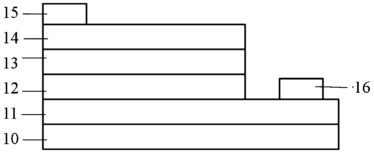
[0035] The present invention also provides a method for preparing an Al-free pWp barrier type antimonide superlattice infrared detector, which may include the following steps:
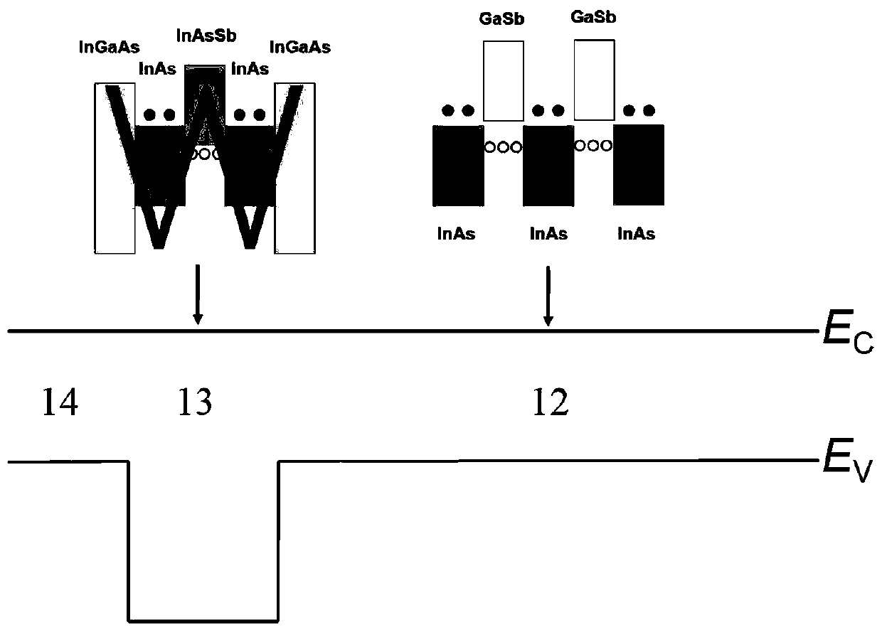
[0036] S1, choose any one of metal-organic chemical vapor deposition and molecular beam epitaxy, and epitaxially grow the p-type InAs / GaSb superlattice lower contact layer 11 and the p-type InAs / GaSb supercrystal on the GaSb or InAs substrate 10 in sequence Lattice absorption layer 12, InGaAs / InAs / InAsSb / InAs / InGaAs superlattice barrier layer 13, and p-type InAs / GaSb superlattice upper contact layer 14.
[0037] S2: Fabricate the mesa on the epitaxial wafer, and deposit a dielectric film to passivate the mesa and sidewall. The mesa is fabricated by any one of wet etching, inductively coupled plasma etching, or reactive ion etching; the dielectric passivation film is formed by plasma enhanced chemical vapor deposition.
[0038] S3: Finally, the electron beam evaporation process is used to deposit the l...
Embodiment 1
[0042] Using Metal Organic Chemical Vapor Deposition (MOCVD) as a growth process, an InAs substrate 10 is provided, and the growth sources are TEGa, TMIn, TMSb and AsH 3 , the p-type dopant source is DEZn. The growth temperature is about 500°C, and the reaction chamber pressure is 100 Torr. After high temperature treatment to remove impurities on the surface of the substrate, according to figure 1 The IR detector structure shown is grown sequentially:
[0043] (1) 100 alternating periods of InAs / GaSb superlattice lower contact layer 11, InAs thickness 4.8nm, GaSb thickness 2.4nm, ie total thickness 0.72μm, Zn doped in InAs and GaSb, the average concentration is 2×10 18 cm -3 ;
[0044] (2) 250 alternating periods of InAs / GaSb superlattice absorption layer 12, the thickness of InAs is 4.8nm, the thickness of GaSb is 2.4nm, that is, the total thickness is 1.8μm, Zn is doped in InAs and GaSb, and the average concentration is 2×10 17 cm -3 ;
[0045] (3) 150 alternating per...
Embodiment 2
[0051] Using molecular beam epitaxy (MBE) as a growth process, a GaSb substrate 10 is provided, the growth source is solid single source Ga, In, As and Sb, and the p-type dopant source is Be. The growth temperature is about 400°C. After the substrate is degassed and impurity removed, according to the following figure 1 The IR detector structure shown is grown sequentially:
[0052] (1) 250 alternating periods of InAs / GaSb superlattice lower contact layer 11, InAs thickness 4.5nm, GaSb thickness 2.1nm, that is, the total thickness 1.65μm, Be doped in InAs and GaSb, the average concentration is 5×10 17 cm -3 ;
[0053] (2) 800 alternating periods of InAs / GaSb superlattice absorption layer 12, InAs thickness 4.5nm, GaSb thickness 2.1nm, that is, the total thickness 5.28μm, Be doped in InAs and GaSb, the average concentration is 5×10 16 cm -3 ;
[0054] (3) 250 alternating periods of InGaAs / InAs / InAsSb / InAs / InGaAs superlattice barrier layer 13, wherein the Ga component in In...
PUM
 Abstract
Description
Claims
Application Information

