
A Polishing Method Combining Electrolytic Polishing and Chemical Mechanical Polishing for Aluminum Nitride Single Wafer

An electrolytic polishing and chemical mechanical technology, applied in grinding/polishing equipment, circuits, grinding machine tools, etc., can solve the problems of few polishing methods, scratches on the wafer surface, poor wafer quality, etc., and achieve simple polishing process, The effect of less polishing damage and shorter polishing time

Active Publication Date: 2019-05-24
CHINA ELECTRONICS TECH GRP NO 46 RES INST
View PDF4 Cites 0 Cited by
  • Summary
  • Abstract
  • Description
  • Claims
  • Application Information

AI Technical Summary

Problems solved by technology

Aluminum nitride single crystal is a hard and brittle material with stable chemical properties. It is not easy to react with acid and alkali at room temperature. At present, there are not many researches on the polishing method of aluminum nitride single wafer. The silicon sol commonly used in the semiconductor wafer polishing method is used for chemical mechanical The removal rate of polished (CMP) wafers is low, there are still scratches or unevenness on the surface of the wafer after polishing, and the quality of the wafer after polishing is not good

Method used


Image

  • A Polishing Method Combining Electrolytic Polishing and Chemical Mechanical Polishing for Aluminum Nitride Single Wafer
  • A Polishing Method Combining Electrolytic Polishing and Chemical Mechanical Polishing for Aluminum Nitride Single Wafer

Examples


Embodiment 1

[0026] The first step, electrolytic polishing;

[0027] For electropolishing, a 10mm×10mm aluminum nitride wafer was placed on the anode, lead was used as the cathode, and the electrolysis temperature was controlled at 20°C. Polishing fluid and related parameters are as follows:

[0028] Electropolishing fluid ratio: 6g sulfamic acid (NH 2 SO 3 H) + 1g oxalic acid (H 2 C 2 o 4 )+1.5gEDTA+91.5g deionized water.

[0029] Polishing parameters: pulsed DC power supply voltage 25V, working ratio 1:10, pulse frequency 1.6Hz, current density 5A / dm 2 , stirring speed 3r / s, polishing time 5min.

[0030] The second step, chemical mechanical polishing;

[0031] Clean the wafer obtained by electrolytic polishing, and paste it evenly on the ceramic plate for chemical mechanical polishing. The polishing liquid and related parameters are as follows:

[0032] Polishing liquid: 20g of potassium dichromate (Na 2 Cr 2 o 7 ), 2g ammonium sulfate ((NH 4 ) 2 SO 4 ) and 77g of deionize...

Embodiment 2

[0036]The first step, electrolytic polishing;

[0037] For electropolishing, a 10mm×10mm aluminum nitride wafer was placed on the anode, lead was used as the cathode, and the electrolysis temperature was controlled at 20°C. Polishing fluid and related parameters are as follows:

[0038] Electropolishing fluid ratio: 7g sulfamic acid (NH 2 SO 3 H)+0.5g oxalic acid (H 2 C 2 o 4 )+0.5gEDTA+92g deionized water.

[0039] Polishing parameters: pulsed DC power supply voltage 45V, working ratio 1:4, pulse frequency 3.0Hz, current density 15A / dm 2 , stirring speed 3r / s, polishing time 5min.

[0040] The first step, chemical mechanical polishing;

[0041] Clean the wafer obtained by electrolytic polishing, and paste it evenly on the ceramic plate for chemical mechanical polishing. The polishing liquid and related parameters are as follows:

[0042] Polishing liquid: 16g of potassium dichromate (Na 2 Cr 2 o 7 ), 6g ammonium sulfate ((NH 4 ) 2 SO 4 ) and 74g of deionized wa...


PUM

PropertyMeasurementUnit
surface roughnessaaaaaaaaaa

Abstract

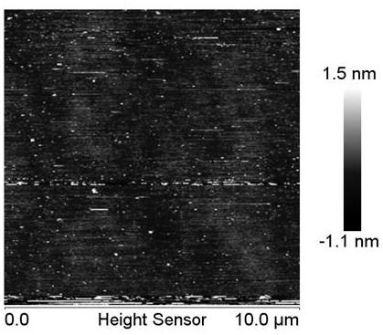
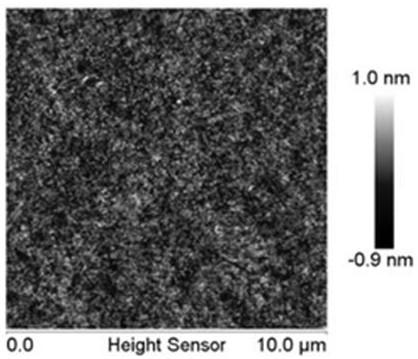
The invention discloses an aluminum nitride single crystal wafer electrolytic polishing and chemical mechanical polishing combined polishing method. An electrolytic polishing solution is made of raw materials including 6 to 7% of sulfamic acid, 0.5 to 1% of oxalic acid, 0.5 to 1.5% of EDTA and 91.5 to 92% of deionized water. After electrolytic polishing is carried out, quartz wax is used for pasting an aluminum nitride single crystal wafer to a ceramic disc, a blade is used for scraping a small amount of wax flowing out of the edge of the wafer, and cleaning is achieved through alcohol; a chemical mechanical polishing solution is made of raw materials including, by weight percent, 16 to 20% of potassium dichromate, 2 to 6% of ammonium sulfate, 0.2 to 4% of nitric acid or sulfuric acid or phosphoric acid and 74 to 77% of deionized water. In the polishing process, an adopted polishing pad is a non-woven polishing cloth. After machining through the method, the wafer surface achieves global planarizartion, no scratch and uneven condition exists, the surface roughness Ra is smaller than or equal to 0.2 nm, and the whole net processing time can be shortened to be within one hour.

Description

technical field [0001] The invention designs a polishing method for combining electrolytic polishing and chemical mechanical polishing of an aluminum nitride single wafer, and belongs to the processing field of semiconductor materials. Background technique [0002] Aluminum nitride (AlN) single crystal has a large band gap, high breakdown field strength, high thermal conductivity, good thermal stability, and is completely transparent in the DUV band of visible light. It has broad applications in the fields of microelectronics and optoelectronics. Application prospect. [0003] AlGaN / GaN high-mobility transistor (HEMT) materials and devices exhibit excellent performance in high-frequency applications, especially for next-generation microwave power devices. [0004] Aluminum nitride single wafers need to undergo a wafer polishing process before application to remove the surface damage of the wafer after grinding. Aluminum nitride single crystal is a hard and brittle material...

Claims


Application Information

Patent Timeline
Patent Type & Authority Patents(China)
IPC IPC(8): B24B37/10B24B57/02H01L21/304C25F3/30
CPCB24B37/10B24B57/02C25F3/30H01L21/304
Inventor 徐世海李晖高飞程红娟金雷张丽
Owner CHINA ELECTRONICS TECH GRP NO 46 RES INST
Learn More