A kind of tizn alloy film and its preparation method and application
A technology of alloy film and dielectric film is applied in the field of functional film preparation, which can solve the problems of waste pollution, high cost, and complicated methods.
- Summary
- Abstract
- Description
- Claims
- Application Information
AI Technical Summary
Problems solved by technology
Method used
Image
Examples
Embodiment 1
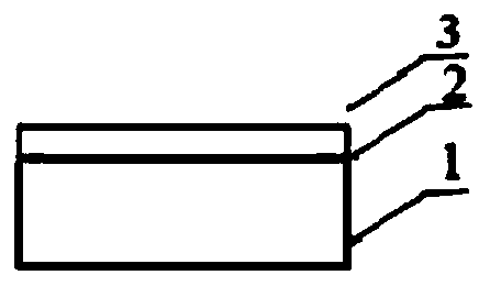
[0081] The present embodiment provides a kind of preparation method of TiZn alloy film, and its specific method is:
[0082] (1) Place the cleaned n-Si (100) substrate on the arched workpiece frame of the electron beam evaporation equipment, place the magnesium fluoride film material with a purity of 99.9% in a graphite crucible as an evaporation source, and the substrate temperature is 100 ℃, the background vacuum is 3×10 - 6 torr, high voltage 10Kv, beam current 35mA, deposition rate The thickness of the magnesium fluoride dielectric film is 100nm, and the deposition rate and film thickness are monitored online in real time by a quartz crystal film thickness meter;
[0083] (2) Place the substrate prepared in step (1) on the substrate stage of the magnetron sputtering system, use the ultra-pure zinc target with a purity of 99.99% and the ultra-pure titanium target with a purity of 99.99% as the sputtering source, and use ultra-pure argon gas As the working gas to prepare...
Embodiment 2
[0090] This embodiment provides a kind of preparation method of TiZn alloy film, and its specific method refers to embodiment 1, difference is:
[0091] In step (1), the thickness of the magnesium fluoride dielectric film is 150nm; in step (2), the radio frequency power of the titanium target is 80w.
[0092] The TiZn alloy film prepared in this example is composed of nano-column structure, the diameter of the nano-column is about 40nm, the height of the nano-column is about 75nm, and the spacing of the nano-column is about 14nm. The atomic ratio of Ti and Zn is shown in Table 1. The TiZn alloy film prepared in this embodiment has super strong electric field coupling effect.
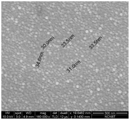
[0093] Fig. 4 (a) is the scanning electron microscope surface topography figure of the TiZn alloy film sample prepared in this embodiment, marked the diameter of the nanocolumn on some positions in this sample among the figure, as can be seen from this figure, this embodiment The diameter of the nanocol...
Embodiment 3
[0096] This embodiment provides a kind of preparation method of TiZn alloy film, and its specific method is with reference to embodiment 2, and difference is: in step (1), magnesium fluoride dielectric film thickness is 250nm, and dielectric film deposition rate is The deposition temperature is 150° C.; in step (2), the deposition time of the TiZn alloy film is 50 min (twice the deposition time of Example 2).
[0097] The TiZn alloy film prepared in this example is composed of nano-column structure, the diameter of the nano-column is about 50nm, the height of the nano-column is about 146nm, and the spacing of the nano-column is about 15nm. The atomic ratio of Ti and Zn is shown in Table 1. The TiZn alloy film prepared in this embodiment has super strong electric field coupling effect.
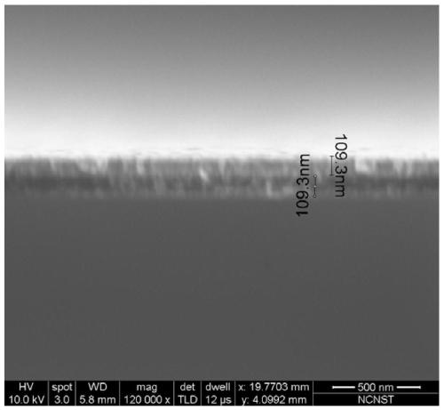
[0098] Figure 5 The scanning electron microscope sectional view of the TiZn alloy film sample prepared for this example, the thickness of the magnesium fluoride dielectric film marked in the...
PUM
| Property | Measurement | Unit |
|---|---|---|
| diameter | aaaaa | aaaaa |
| height | aaaaa | aaaaa |
| thickness | aaaaa | aaaaa |
Abstract
Description
Claims
Application Information


