One-dimensional organic semiconductor nano material and preparation method and application thereof

A technology of organic semiconductors and nanomaterials, applied in the field of organic semiconductor nanomaterials and their preparation, can solve the problems of specific detection of phosgene organic semiconductor nanomaterials that have not been reported, achieve excellent photoelectric properties and chemical stability, and improve sensitivity strong photochemical stability

Inactive Publication Date: 2018-09-28
YANGTZE NORMAL UNIVERSITY
View PDF4 Cites 9 Cited by
  • Summary
  • Abstract
  • Description
  • Claims
  • Application Information

AI Technical Summary

Problems solved by technology

However, no organic semiconductor nanomaterials that specifically detect phosgene have been reported so far.

Method used


Image

  • One-dimensional organic semiconductor nano material and preparation method and application thereof
  • One-dimensional organic semiconductor nano material and preparation method and application thereof
  • One-dimensional organic semiconductor nano material and preparation method and application thereof

Examples


preparation example Construction

[0043] 2. The preparation method of one-dimensional organic semiconductor nanomaterials, comprising the following steps: dissolving the building monomer in a benign solvent, fully dissolving, then adding a poor solvent, standing for 1-3 days, and sucking out the precipitated flocs , when the organic solvent volatilizes naturally, one-dimensional organic semiconductor nanomaterials can be obtained. The monomers are self-assembled in a mixture of a poor solvent and a good solvent through intermolecular π-π interactions to obtain a one-dimensional organic semiconductor material with high fluorescence quantum yield. The above-mentioned one-dimensional organic nanometer material is dispersed in a poor solvent to form a porous membrane with a network structure.

[0044] The volume ratio of the good solvent to the poor solvent is 1:5-1:20; the good solvent is chloroform; the poor solvent is ethanol, ether, n-hexane or n-pentane.

[0045] The length of the one-dimensional organic nan...

Embodiment 1 1

[0063] Embodiment 1 The preparation method of a one-dimensional organic semiconductor nanostructure monomer, specifically comprising the following steps:

[0064] (1) Preparation of intermediate compound B

[0065] Take 100mg of 3,4,9,10-perylenetetracarboximide molecule A and 10g of imidazole and heat to 130°C, then add 80mg of 5-aminononane, react for 1h, then add 500mL of ethanol and 10mL of 36 % concentrated hydrochloric acid, stirred overnight, solids were precipitated, the product was suction filtered to collect the solids, and then the solids were washed to neutrality, and finally the intermediate compound B was obtained after rotary evaporation under reduced pressure.

[0066] (2) Preparation of intermediate compound E

[0067] Dissolve 223mg of compound C and 183mg of compound D in 10mL of dichloromethane solvent, then add 202mg of triphenylphosphine and 200mg of diisopropyl azodicarboxylate, react at room temperature for 2h, add 10mL of water to quench the reaction ...

Embodiment 2

[0076] The preparation method of embodiment 2 one-dimensional organic semiconductor nanomaterials

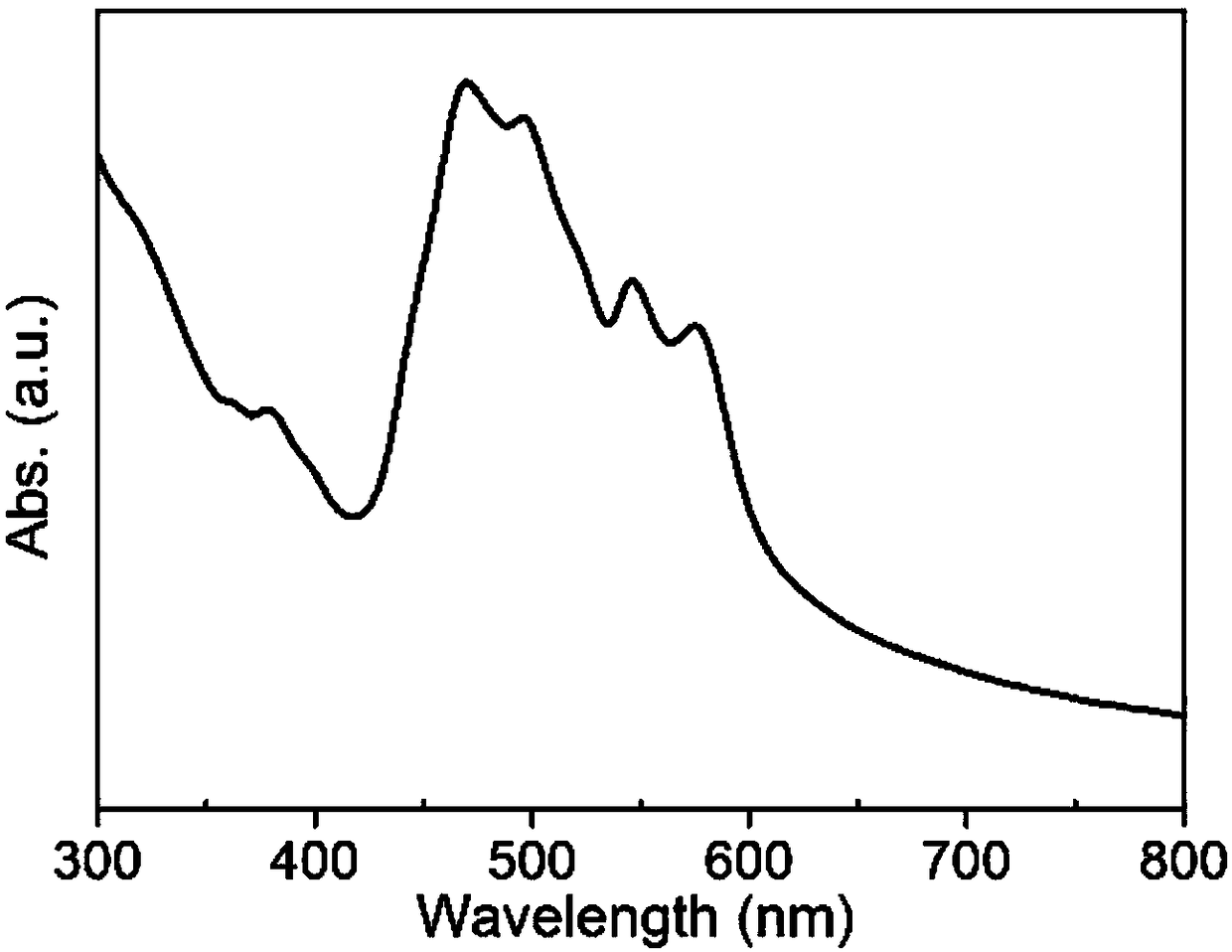
[0077] Take 0.1 mg of the one-dimensional organic semiconductor nano-construction monomer prepared in Example 1, dissolve it in 10 mL of chloroform, shake it evenly, then add 50 mL of ethanol, and let it stand for 3 days. The floc solid is precipitated in the solution, and the obtained floc is removed with a straw. The solid was placed on a clean glass sheet, and after the ethanol evaporated naturally, the one-dimensional organic semiconductor nanomaterial was obtained.


PUM

PropertyMeasurementUnit
lengthaaaaaaaaaa
widthaaaaaaaaaa
wavelengthaaaaaaaaaa

Abstract

The invention discloses a one-dimensional organic semiconductor nano material and a preparation method and an application thereof. The material employs a unsymmetrical perylene bisimide derivative monomer as a construction monomer, hydrophilic branched-chain alkyl (5-nonane) and pentafluorophenyl substituent are respectively introduced at two sides of perylene bisimide, and the one-dimensional organic semiconductor nano material can be obtained by self assembly preparation through Pi-Pi interacting of construction monomers. The one-dimensional organic semiconductor nano-material has the advantages of high fluorescence quantum yield, porous performance, large surface area, and good stability, greatly reduces the detection lowest limitation, has good anti-interference capability for an aggregate such as triphosgene and other common gases and organic solvent steam, and realizes specific and high-sensitivity detection on phosgene.

Description

technical field [0001] The invention belongs to the field of organic semiconductor materials, and in particular relates to a one-dimensional organic semiconductor nanometer material and its preparation method and application. Background technique [0002] Phosgene (COCl 2 ), the chemical name is dichlorocarbonyl, which is an important combat agent in lethal chemical weapons and one of the chemical poisons threatened by chemical terrorism. At the same time, phosgene is also an important chemical raw material, which is widely used in the fields of polymer materials, pesticides, medicines, spices and dyes, especially for the synthesis of engineering plastics polycarbonate and polyurethane raw materials with excellent performance. Because phosgene is an acid chloride compound, the active group is a carbonyl group, its chemical properties are very active, and it is easy to react with nucleophiles, such as important functional groups such as amino, sulfhydryl, and hydroxyl groups...

Claims


Application Information

Patent Timeline
Patent Type & Authority Applications(China)
IPC IPC(8): C07D471/06G01N21/64
CPCC07D471/06G01N21/6402G01N21/6428G01N21/643G01N2021/6432
Inventor 张义斌刘晓玲胡艳勇
Owner YANGTZE NORMAL UNIVERSITY
Why Eureka
Try Eureka