Raw material sintering process of silicon carbide crystals grown by PVT (physical vapor deposition) method

A technology of silicon carbide and raw materials, applied in crystal growth, single crystal growth, single crystal growth, etc., can solve the problems of reduced sublimation decomposition rate of silicon carbide powder source, reduced growth rate of silicon carbide crystal, and reduced effective transportation efficiency, etc. Achieve the effects of weakening crystallization, reducing radial temperature gradient, and increasing average growth rate

Inactive Publication Date: 2018-10-09
FUJIAN NORSTEL MATERIAL TECH CO LTD
View PDF9 Cites 6 Cited by
  • Summary
  • Abstract
  • Description
  • Claims
  • Application Information

AI Technical Summary

Problems solved by technology

[0007] The purpose of the present invention is to overcome the deficiencies of the prior art, to provide a raw material sintering process for silicon carbide crystals grown by PVT method, through the sintering treatment of silicon carbide raw materials, to improve the thermal field distribution of silicon carbide crystals grown by PVT method The resulting densification of silicon carbide powder source, delamination and gradual decomposition of individual silicon carbide particles make the process of preparing silicon carbide crystals by sublimation method, as the crystal growth continues, the effective transport efficiency of gas phase substances to the crystal growth surface decreases, and at the same time The sublimation decomposition rate of silicon carbide powder source gradually decreases, which leads to the gradual decrease or even stop of the growth rate of silicon carbide crystal

Method used


Image

  • Raw material sintering process of silicon carbide crystals grown by PVT (physical vapor deposition) method
  • Raw material sintering process of silicon carbide crystals grown by PVT (physical vapor deposition) method

Examples


Embodiment 1

[0035] A raw material sintering process for silicon carbide crystals grown by PVT method

[0036] The process steps are as follows:

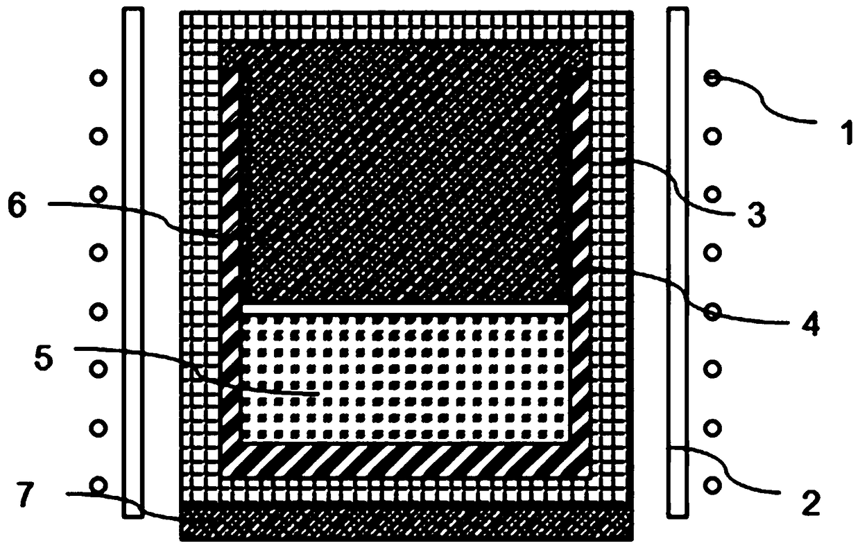
[0037] S10, put 1.0kg of silicon carbide raw material with a purity of 5N into a graphite crucible with a thickness of 5mm, flatten it, put it into a sintering fixture, the distance between the bottom of the sintering fixture and the upper surface of the silicon carbide raw material is 5mm, and wrap the outer circumference of the graphite crucible with a layer thickness 10mm thermal insulation layer;

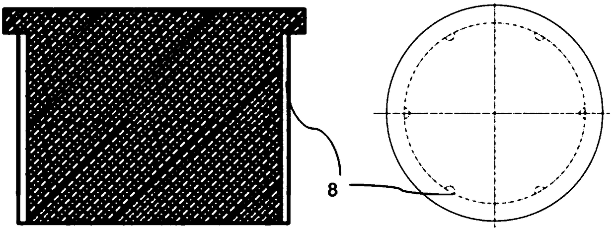
[0038] In the above operations, the silicon carbide raw material can also be a mixture of high-purity carbon powder and silicon powder; the graphite crucible also includes a bottom heating plate made of high-density graphite with a thickness of 10mm and a diameter 10mm larger than that of the graphite crucible; IG310 with six vias.

[0039] S20, evacuate the graphite crucible to a pressure of 5x10 -2 mbar, filled with argon to control the press...

Embodiment 2

[0043] A raw material sintering process for silicon carbide crystals grown by PVT method

[0044] The process steps are as follows:

[0045] S10, put 1.4kg of silicon carbide raw material with a purity of 6N into a graphite crucible with a thickness of 20mm, flatten it, put it into a sintering fixture, the distance between the bottom of the sintering fixture and the upper surface of the silicon carbide raw material is 40mm, and wrap the graphite crucible with 4 layers of thickness 5mm heat insulation layer;

[0046] In the above operations, the silicon carbide raw material can also be a mixture of high-purity carbon powder and silicon powder; the graphite crucible also includes a bottom heating plate made of high-density graphite with a thickness of 30 mm and a diameter 100 mm larger than that of the graphite crucible; IG310 with six vias.

[0047] S20, evacuate the graphite crucible to a pressure of 4x10 -2 mbar, filled with argon gas to control the pressure at 500mbar, use ...

Embodiment 3

[0051] A raw material sintering process for silicon carbide crystals grown by PVT method

[0052] The process steps are as follows:

[0053] S10, put 1.2kg of silicon carbide raw material with a purity of 5N into a graphite crucible with a thickness of 20mm, flatten it, put it into a sintering fixture, the distance between the bottom of the sintering fixture and the upper surface of the silicon carbide raw material is 20mm, and wrap the graphite crucible with 4 layers of thickness 6mm heat insulation layer;

[0054] In the above operations, the silicon carbide raw material can also be a mixture of high-purity carbon powder and silicon powder; the graphite crucible also includes a bottom heating plate made of high-density graphite with a thickness of 20 mm and a diameter 50 mm larger than that of the graphite crucible; IG310 with six vias.

[0055] S20, evacuate the graphite crucible to a pressure of 3x10 -2 mbar, filled with argon gas to control the pressure at 200mbar, use...


PUM

PropertyMeasurementUnit
thicknessaaaaaaaaaa
thicknessaaaaaaaaaa

Abstract

The invention discloses a raw material sintering process of silicon carbide crystals grown by a PVT (physical vapor deposition) method. The silicon carbide raw material is led to the sintering processwith the PVT method, a sintering fixture is designed, the silicon carbide is sintered through the previously designed sintering fixture, and the silicon carbide crystals are grown by the PVT method.The raw material sintering process has the advantages that the silicon carbide raw material forms a certain structure through sintering of the silicon carbide raw material, crystallization of the silicon carbide raw material is weakened, densification degree of the silicon carbide raw material is lowered, impurities carried in the silicon carbide raw material can be removed during sintering, fullsublimation and stable growth speed of the silicon carbide crystals by the PVT method can be effectively controlled and maintained, and the yield of the utilization of the silicon carbide raw materialand the silicon carbide crystals is increased.

Description

technical field [0001] The invention relates to the technical field of silicon carbide crystal growth, in particular to a raw material sintering process for silicon carbide crystals grown by a PVT method. Background technique [0002] With the development of new energy vehicles and the promotion of 5G mobile phone network, the silicon carbide market is getting bigger and bigger. Silicon carbide single crystal material is the representative of the third generation wide bandgap semiconductor material, which has the characteristics of wide bandgap, high thermal conductivity, high breakdown electric field, high radiation resistance, etc. SiC devices can be used in artificial satellites, rockets, radar and communications, Aerospace vehicles, marine exploration, earthquake prediction, oil drilling, machining and automotive electronics and other important fields. [0003] At present, physical vapor deposition (PVT) is the main growth method for silicon carbide single crystal growt...

Claims


Application Information

Patent Timeline
Patent Type & Authority Applications(China)
IPC IPC(8): C30B35/00C04B35/64C30B23/00C30B29/36
CPCC04B35/64C30B23/00C30B29/36C30B35/007
Inventor 陈华荣张洁廖弘基蔡如腾
Owner FUJIAN NORSTEL MATERIAL TECH CO LTD
Why Eureka
Try Eureka