Manufacturing method of organic electroluminescence element and organic electroluminescence element

The technology of an electroluminescent element and a manufacturing method is applied in the manufacture of organic electroluminescent elements and the field of organic electroluminescent elements, and can solve problems such as inability to reduce manufacturing costs, lower output, deformation of flexible substrates, etc.

Active Publication Date: 2021-03-30
MERCK PATENT GMBH
View PDF21 Cites 0 Cited by
  • Summary
  • Abstract
  • Description
  • Claims
  • Application Information

AI Technical Summary

Problems solved by technology

[0009] However, in the technology described in the above-mentioned Patent Document 2, high-temperature and long-term post-treatment is required after coating and film formation, and without post-treatment, further layers cannot be laminated on this layer.
In addition, not only energy and time are required for post-processing, but also flexible substrates are deformed by this energy, so there is a problem that the yield is reduced and the manufacturing cost cannot be reduced.
[0010] Furthermore, in the technique described in the above-mentioned Patent Document 3, even after the materials in the mixed layer are separated, mixing due to contact between the light-emitting material and the electron-transport material cannot be avoided, so there is a gap between the light-emitting material and the electron-transport material. Ligand exchange and complex formation occur between them, resulting in quenching and degradation of device performance
In addition, since it is necessary to carry out molecular design for various materials, there is a problem that the design of the entire layer is difficult.

Method used


Image

  • Manufacturing method of organic electroluminescence element and organic electroluminescence element
  • Manufacturing method of organic electroluminescence element and organic electroluminescence element
  • Manufacturing method of organic electroluminescence element and organic electroluminescence element

Examples


Embodiment 1

[0277] "Preparation of Organic EL Element 101"

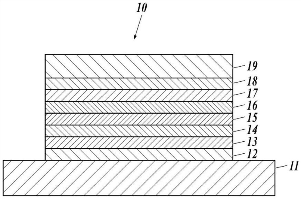
[0278] Anode / hole injection layer / hole transport layer / light emitting layer / blocking layer / electron transport layer / electron injection layer / cathode are laminated and sealed on a base material as follows to prepare a bottom emission type organic EL element 101 .

[0279] (preparation of base material)

[0280] First, on the entire surface of a polyethylene naphthalate film (manufactured by Teijin DuPont Co., Ltd., hereinafter abbreviated as PEN) on which the anode is formed, atmospheric pressure plasma having the structure described in JP-A-2004-68143 is used. discharge treatment device, formed containing SiO x Inorganic gas barrier layer, and make the layer thickness 500nm. Thus, the oxygen transmission rate of 0.001mL / (m 2 24h) or less, the water vapor transmission rate is 0.001g / (m 2 24h) or less flexible substrates having gas barrier properties.

[0281] (formation of anode)

[0282] ITO (Indium Tin Oxide) with a thick...

Embodiment 2

[0345] "Preparation of Organic EL Element 201"

[0346] In the preparation of the organic EL element 101 in Example 1 above, except that the material contained in the coating solution for barrier layer formation was changed to HS-12, the organic EL element 201 was prepared in the same manner.

[0347] "Preparation of Organic EL Element 202"

[0348] In the production of the organic EL element 101 of the above-mentioned Example 1, the organic EL element 202 was produced in the same manner except that the formation method of the barrier layer was changed as described below.

[0349] (formation of barrier layer)

[0350] The substrate on which the light-emitting layer was formed was placed in a vacuum evaporation apparatus without being exposed to the atmosphere. In addition, put HS-12 into a molybdenum resistance heating boat and load it into a vacuum evaporation device, and depressurize the vacuum chamber to 4×10 -5 After Pa, the boat was energized and heated, and HS-12 was ...

Embodiment 3

[0358] "Preparation of Organic EL Element 301"

[0359] In the preparation of the organic EL element 101 in Example 1 above, except that the material contained in the coating solution for barrier layer formation was changed to HS-2, the organic EL element 301 was prepared in the same manner.

[0360] "Preparation of Organic EL Element 302 and Organic EL Element 303"

[0361] In the preparation of the organic EL element 101 of Example 1 above, the materials contained in the coating liquid for barrier layer formation were changed to those shown in Table 5, and the method of forming the electron transport layer was changed to the following, except Otherwise, the organic EL element 302 and the organic EL element 303 were produced in the same manner.

[0362] (Formation of electron transport layer)

[0363] The substrate on which the barrier layer was formed was loaded into a vacuum evaporation apparatus without being exposed to the atmosphere. In addition, compound A was put into...


PUM

PropertyMeasurementUnit
solubility (mass)aaaaaaaaaa
glass transition temperatureaaaaaaaaaa
thicknessaaaaaaaaaa

Abstract

It is an object of the present invention to provide a method for manufacturing an organic EL element having high luminous efficiency and long life at low cost, which is applicable to flexible substrates. This method of manufacturing an organic EL element is a method of manufacturing an organic EL element 10 having a light emitting layer 15 between an anode 12 and a cathode 19, a blocking layer 16, and an electron transport layer 17, by using The barrier layer 16 is formed from a coating solution containing a compound having a structure represented by the following general formula (1) and a polar fluorinated solvent. [X means O, S or NR 9 . R 1 ~R 9 each represent a hydrogen atom, a substituent, or a substituent represented by the general formula (2), and at least one represents a substituent represented by the general formula (2)]. [L represents a linking group, R represents a substituent, and at least one of L and R represents an alkylene group or an alkyl group].

Description

technical field [0001] The present invention relates to a manufacturing method of an organic electroluminescent element and an organic electroluminescent element. In particular, the present invention relates to a method for manufacturing an organic electroluminescent element having high luminous efficiency and long life, which can be used on a flexible substrate and at low cost, and the organic electroluminescent element. Background technique [0002] Conventionally, an organic electroluminescence (electroluminescence: hereinafter also referred to as "organic EL") element can be cited as a light-emitting electronic display device. The organic EL element has a structure in which a light-emitting layer containing a light-emitting compound is sandwiched between a cathode and an anode, and by injecting electrons and holes into the light-emitting layer and recombining them to generate excitons (Exciton), the excitons are used Emit light (fluorescence / phosphorescence) upon inacti...

Claims


Application Information

Patent Timeline
Patent Type & Authority Patents(China)
IPC IPC(8): H05B33/10C09K11/06H01L51/50
CPCC09K11/06H05B33/10H10K50/00H10K85/657H10K85/40H10K71/00
Inventor 及川和博
Owner MERCK PATENT GMBH
Why Eureka
Try Eureka