Deep-ultraviolet photoelectric detector of amorphous gallium oxide-based thin film transistor

A thin-film transistor and gallium oxide-based technology, applied in semiconductor devices, circuits, electrical components, etc., can solve problems such as small detection range, and achieve the effects of strong breakdown resistance, low power consumption, and simple preparation process

Inactive Publication Date: 2019-05-10
NINGBO INST OF MATERIALS TECH & ENG CHINESE ACADEMY OF SCI
View PDF6 Cites 14 Cited by
  • Summary
  • Abstract
  • Description
  • Claims
  • Application Information

AI Technical Summary

Problems solved by technology

However, because the IGZO band gap is small, about 3.0-3.2eV, and the detection wavelength of the corresponding deep ultraviolet photodetector is about 387-413nm, the detection range of the IGZO thin film transistor type deep ultraviolet photodetector is small, and it needs to be filtered out during use. visible light

Method used


Image

  • Deep-ultraviolet photoelectric detector of amorphous gallium oxide-based thin film transistor
  • Deep-ultraviolet photoelectric detector of amorphous gallium oxide-based thin film transistor
  • Deep-ultraviolet photoelectric detector of amorphous gallium oxide-based thin film transistor

Examples


Embodiment 1

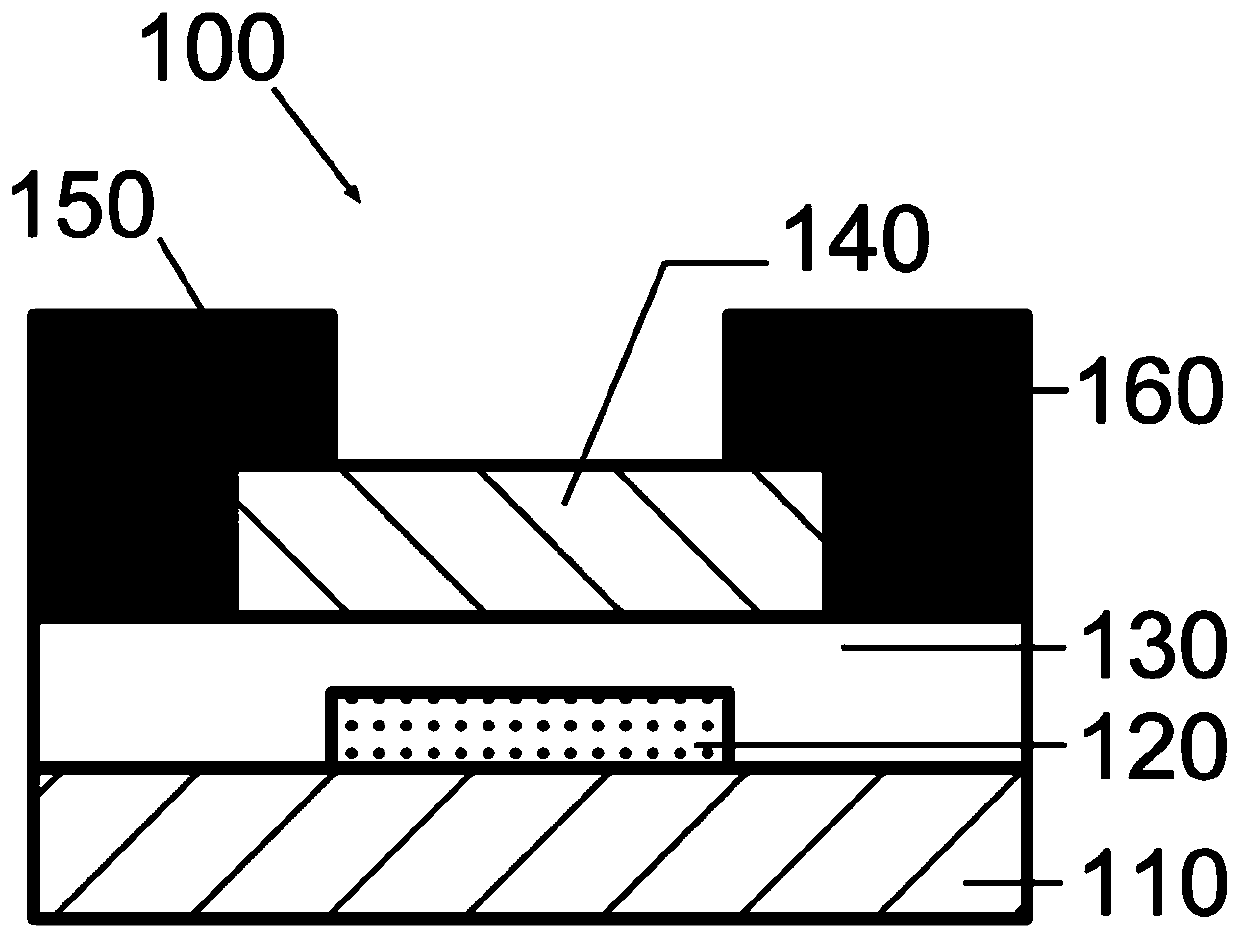
[0049] In this implementation case, firstly through step S110, select p+-Si / SiO 2 (100) Thermally oxidized silicon chip is used as substrate 110, and each ultrasonic cleaning 10min with acetone alcohol deionized water, N 2 Blow dry and set aside.

[0050] Furthermore, through step S120, the following three solutions are configured:

[0051]

[0052] The precursor solution was thoroughly mixed by continuous sonication for four hours at room temperature. After aging for 24 h, filter with a syringe and a 0.22 μm filter to obtain S1, S2, S3 and three precursor solutions.

[0053] Then, through step S130, the surface of the thermally oxidized silicon wafer is cleaned with plasma to increase the hydrophilicity of the surface, the power is 100W, and the time is 2 minutes.

[0054] In the next step, through step S140 , the above prepared precursor solution is spin-coated on the thermally oxidized silicon wafer to form the channel layer 140 . The spin-coating speed is 3000 rpm, ...

Embodiment 2

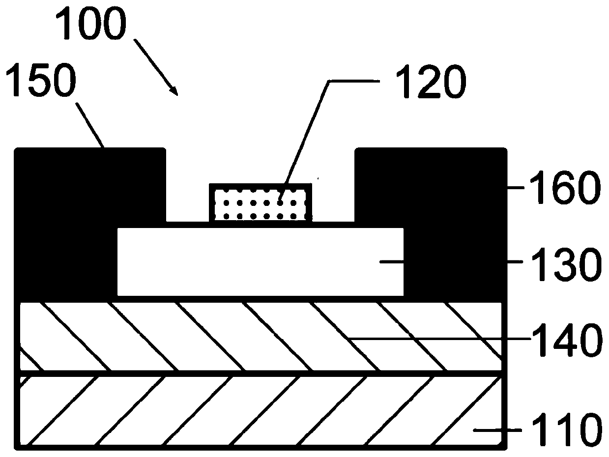
[0061] In this implementation case, firstly through step S210, select p+-Si / SiO 2 (100) Thermally oxidized silicon chip is used as substrate 110, and each ultrasonic cleaning 10min with acetone alcohol deionized water, N 2 Blow dry and set aside.

[0062] Furthermore, through step S220, configure the following three solutions

[0063]

[0064] The precursor solution was thoroughly mixed by continuous sonication for four hours at room temperature. After aging for 24 h, it was filtered with a syringe and a 0.22 μm filter to obtain three precursor solutions of S4, S5 and S6.

[0065] Then, through step S230, the surface of the thermally oxidized silicon wafer is cleaned with plasma to increase the hydrophilicity of the surface, the power is 100W, and the time is 2 minutes.

[0066] In the next step, through step S240 , the above prepared precursor solution is spin-coated on the thermally oxidized silicon wafer to form the channel layer 140 . The spin-coating speed is 3000 ...

Embodiment 3

[0073] For the thin-film transistor deep-ultraviolet photodetector provided in Example 2, the Ga content in the solution configured is 0.75. Under the irradiation of deep ultraviolet light, the degree of leftward shift of the transfer curve under visible light irradiation is relatively high, and its ultraviolet-visible suppression ratio All were worse than S1, S4, S5 and S6.


PUM


Abstract

The invention discloses a deep-ultraviolet photoelectric detector of an amorphous gallium oxide-based thin film transistor. The deep-ultraviolet photoelectric detector comprises the thin film transistor, wherein the transistor comprises a substrate, a gate electrode, a gate dielectric layer, a channel layer, a source electrode and a drain electrode, the channel layer is an amorphous gallium oxide-based thin film, the thin film transistor is of a bottom gate structure, the gate electrode is arranged on the substrate, the gate dielectric layer covers the gate electrode, the channel covers an upper part of the gate dielectric layer, the source and the drain are respectively arranged at two ends of the channel layer, or the thin film transistor is of a top gate structure, the channel layer covers the substrate, the gate dielectric layer covers an upper part of the channel layer, the source electrode and the drain electrode are respectively arranged at two ends of the gate dielectric layer,and the gate electrode is arranged on the gate dielectric layer. The deep-ultraviolet photoelectric detector provided by the invention has the advantages of relatively high response and low power consumption under irradiation of deep ultraviolet light (320 nanometers), and moreover, the fabrication method is simple, large-area integration can be achieved, and the deep-ultraviolet photoelectric detector is compatible with a flexible substrate.

Description

technical field [0001] The invention relates to the technical field of semiconductor devices, in particular to a deep ultraviolet photodetector based on an amorphous gallium oxide-based thin film transistor. Background technique [0002] Deep ultraviolet detection technology is another photoelectric detection technology emerging after infrared and laser detection technology. In terms of military, deep ultraviolet detectors can be used in fields such as biochemical analysis, missile guidance, missile early warning, deep ultraviolet communication and flight tracking; in civilian aspects, they can be used in ozone detection, combustion engineering, environmental pollution monitoring, biomedical analysis, etc. field. [0003] At present, semiconductor deep ultraviolet detectors mainly include three types: photoconductive type, Schottky type and PN junction type. For example, the Chinese patent document whose publication number is CN106449857A discloses a kind of ultraviolet ph...

Claims


Application Information

Patent Timeline
Patent Type & Authority Applications(China)
IPC IPC(8): H01L31/113H01L31/0376H01L31/032
Inventor 梁凌燕肖溪曹鸿涛裴郁段宏筱
Owner NINGBO INST OF MATERIALS TECH & ENG CHINESE ACADEMY OF SCI
Why Eureka
Try Eureka