A high threshold voltage normally-off high electron mobility transistor and its preparation method
A technology with high electron mobility and high threshold voltage, which is applied in semiconductor/solid-state device manufacturing, circuits, electrical components, etc., can solve the problem of small gate withstand voltage and threshold voltage, difficulty in controlling the uniformity of gate etching depth, fluorine ion Distributed thermal stability and performance reliability problems are difficult to overcome, and achieve the effect of large conduction current density
- Summary
- Abstract
- Description
- Claims
- Application Information
AI Technical Summary
Problems solved by technology
Method used
Image
Examples
Embodiment 1
[0054] The specific implementation process of this patent application is as follows:
[0055] Step ①: wafer growth.
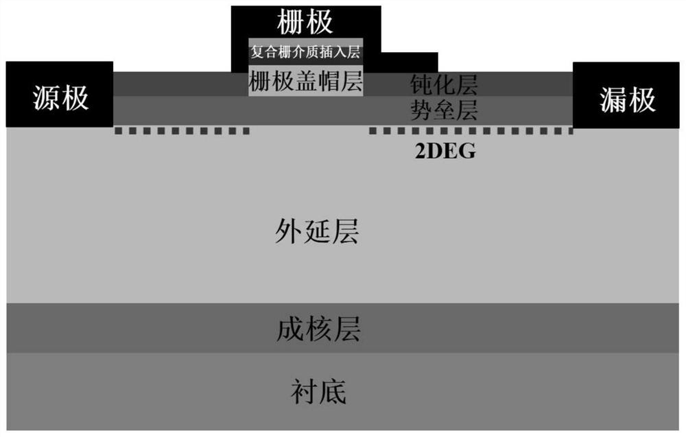
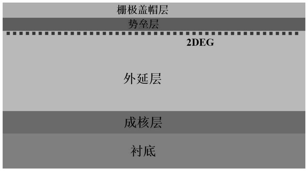
[0056] AlN or AlGaN superlattice nucleation layer, 2-10μm GaN or GaAs epitaxial layer, 5-100nm AlGaN, InAlN, AlN or AlGaAs barrier layer (where the Al composition is 0.05-0.3), 30-100nm p-GaN or p-InGaN or p-AlGaN gate capping layers, such as figure 2 , image 3 shown.
[0057] Step ②: Etching the epitaxial layer structure.
[0058] Use semiconductor lithography technology and etching technology to make device mesas, and use semiconductor etching technologies such as inductively coupled plasma (ICP) or reactive ion etching (RIE) based on Cl-based gases to etch the surface by 300-800nm to achieve Countertop isolation. Repeat this step to etch away the barrier layer in the source and drain regions to form grooves; further etch away the p-type capping layer outside the gate region, such as Figure 4 shown. Among them, the semiconductor photolithography ...
Embodiment 2
[0066] The specific implementation process of this patent application is as follows (detailed parameters and steps):
[0067] Step ①: GaN structure epitaxial growth.
[0068] A 100nm AlGaN superlattice nucleation layer, a 2μm GaN epitaxial layer, a 20nm AlGaN barrier layer (Al composition is 0.25), and a 50nm p-GaN cap were sequentially grown on a 6-inch p-type Si substrate by MOCVD equipment layer. The structure and size of the device are designed as follows: the distance between the source and the gate of the device is 2 μm, the length of the gate is 3 μm, the width is 200 μm, the length of the field plate extending from the gate to the drain is 1 μm, and the distance between the gate and the drain is 10 μm. The electrode area is 200×200μm 2 .
[0069] Step ②: Etching the epitaxial layer structure.
[0070] Using semiconductor lithography technology, the specific process is:
[0071] (1) Evenly spin coat the sample with AZ5214 photoresist at a rate of 4000r / min for 30s;...
PUM
 Abstract
Description
Claims
Application Information


