Epitaxial growth method for reducing interface thermal resistance of gallium nitride high-electron-mobility field-effect transistor

A technology of high electron mobility and epitaxial growth, which is applied in the field of epitaxial growth to reduce the interface thermal resistance of GaN high electron mobility field effect transistors, and can solve the problem of deterioration, unfavorable lateral merging of nucleation layers, and thinning material quality, etc. question

Active Publication Date: 2019-09-06
NO 55 INST CHINA ELECTRONIC SCI & TECHNOLOGYGROUP CO LTD
View PDF4 Cites 9 Cited by
  • Summary
  • Abstract
  • Description
  • Claims
  • Application Information

AI Technical Summary

Problems solved by technology

However, under the conventional aluminum nitride nucleation layer process, the lateral migration length of aluminum atoms is low, which is not conducive to the lateral merger between nucleation layer islands, which leads to many mismatch defects in the nucleation layer, poor surface morphology, and nitrogen The high density of mismatch defects in the Al2 nucleation layer extends to the GaN layer resulting in a higher threading dislocation density in the GaN layer
In addition, gallium nitride is a large mismatch heteroepitaxy, and thinning the thickness of the gallium nitride layer will also deteriorate the quality of its own materials

Method used


Image

  • Epitaxial growth method for reducing interface thermal resistance of gallium nitride high-electron-mobility field-effect transistor
  • Epitaxial growth method for reducing interface thermal resistance of gallium nitride high-electron-mobility field-effect transistor
  • Epitaxial growth method for reducing interface thermal resistance of gallium nitride high-electron-mobility field-effect transistor

Examples


Embodiment

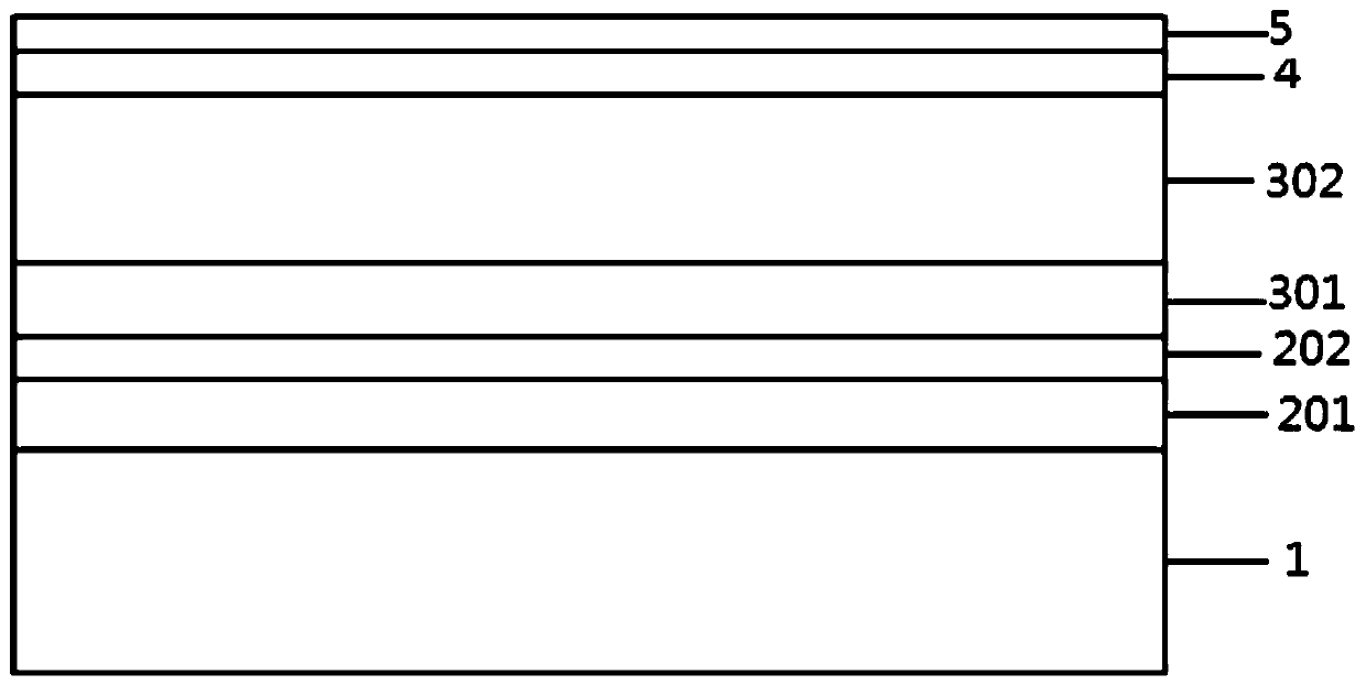
[0039] An epitaxial growth method for reducing the interface thermal resistance of GaN high electron mobility field effect transistors, comprising the following steps:

[0040] (1) Place a 3-inch silicon carbide single crystal substrate on the base of a metal-organic compound chemical vapor deposition (MOCVD) device for epitaxial material growth, set the reaction chamber pressure to 80torr, and the flow rate of hydrogen to 80slm, and the system is heated to 1070°C and maintain the temperature for 8 minutes to remove the contamination on the substrate surface;

[0041] (2) Keep the pressure of the reaction chamber and the flow rate of hydrogen gas constant, continue to heat up to 1140 ° C, feed ammonia gas with a flow rate of 4 slm and keep it for 1 minute, and nitride the substrate;

[0042] (3) keep the reaction chamber pressure, hydrogen flow rate, ammonia flow rate and temperature constant, feed trimethylaluminum with a flow rate of 200 sccm, grow the lower aluminum nitride...


PUM

PropertyMeasurementUnit
thicknessaaaaaaaaaa
thicknessaaaaaaaaaa
thicknessaaaaaaaaaa

Abstract

The invention relates to an epitaxial growth method for reducing interface thermal resistance of a gallium nitride high-electron-mobility field-effect transistor. An epitaxial material is grown through a vapor phase epitaxial growth method of metal organic matter chemical vapor deposition and the like. A gallium nitride epitaxial wafer comprises a substrate, a lower aluminium nitride nucleating layer, an upper aluminium nitride nucleating layer, a gallium nitride transition layer, a gallium nitride buffer layer, a barrier layer and a cap layer from the bottom up in sequence. The carrier gasesused in the growing process of the lower aluminium nitride nucleating layer and the upper aluminium nitride nucleating layer are hydrogen and nitrogen respectively. The carrier gas used in the growingprocess of the gallium nitride transition layer is nitrogen. The carrier gas used in the growing process of the gallium nitride buffer layer is hydrogen or a mixture of hydrogen and nitrogen. Throughthe carrier gas conversion process, the method reduces defect density in the aluminum nitride nucleating layer and the gallium nitride layer, improves interface quality of the aluminum nitride nucleating layer and the gallium nitride layer, and effectively reduces the interface thermal resistance of the gallium nitride high-electron-mobility field-effect transistor.

Description

technical field [0001] The invention belongs to the technical field of semiconductor epitaxial materials, and in particular relates to an epitaxial growth method for reducing the interface thermal resistance of a GaN high electron mobility field effect tube. Background technique [0002] Gallium nitride high electron mobility field effect transistor has the advantages of high output power density, high operating frequency, and radiation resistance. It has unique advantages in the application of microwave power devices, and is developing rapidly in the direction of millimeter wave and high power. Among them, the cut-off frequency has reached 450GHz, and the output power of Ka-band has reached more than 40W. However, in the radio frequency state, a large amount of heat energy is generated near the device channel, which imposes strict requirements on the thermal management capability of the device. However, the performance of current microwave power devices is limited by the i...

Claims


Application Information

Patent Timeline
Patent Type & Authority Applications(China)
IPC IPC(8): H01L21/02
CPCH01L21/02378H01L21/02458H01L21/02502H01L21/0254H01L21/0262H01L29/66462
Inventor 李忠辉彭大青李传皓
Owner NO 55 INST CHINA ELECTRONIC SCI & TECHNOLOGYGROUP CO LTD
Why Eureka
Try Eureka