A miniature spectrum testing system and testing method
A spectroscopic testing and miniature technology, applied in the field of spectral analysis, can solve the problems of limited spectral resolution, low correlation, narrow working wavelength range, etc., to achieve the effect of enhancing photoelectric conversion, realizing performance, and increasing working wavelength range.
- Summary
- Abstract
- Description
- Claims
- Application Information
AI Technical Summary
Problems solved by technology
Method used
Image
Examples
Embodiment 1
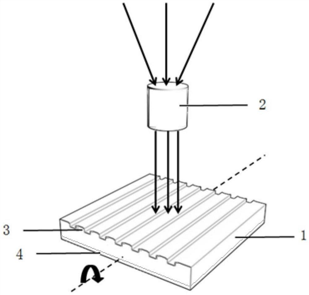
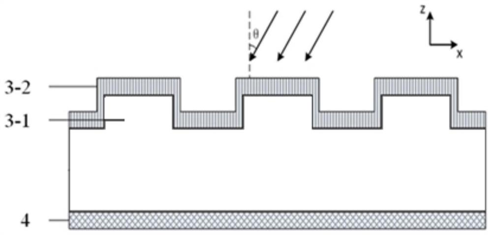
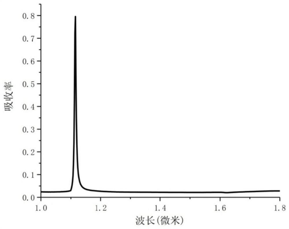
[0042] refer to figure 2 As shown in the figure, this embodiment provides a miniature spectral testing system, where a rotatable silicon wafer faces the first surface of the beam collimation module to form a one-dimensional silicon grating 3-1, wherein the period is 1.1 microns, and the width of the silicon grating is 0.5 Micron, the depth of the silicon grating is 35 nanometers; the silicon grating is covered with a gold film 3-2 with a thickness of 60 nanometers. The silicon grating and the gold film together form a grating and form a Schottky junction. The gold film is used as the first electrode of the photoelectric detection module, and the second electrode 4 of the photoelectric detection module is formed on the second surface of the silicon wafer backlight, which is made of gold material. Thickness 200 nanometers.
[0043] Incident light of different wavelengths resonates with the surface plasmon wave of the grating at a specific incident angle, and the resonance cond...
Embodiment 2
[0051] Figure 10 It is a schematic cross-sectional structure diagram of the photoelectric detection module of the micro-spectroscopy test system of the present embodiment. As shown in the figure, the photoelectric detection module in this embodiment is prepared by covering the surface of the silicon wafer with a gold film, and then forming a silicon dioxide grating 3-3 on the gold film, wherein the thickness of the gold film is 80 nanometers, and the silicon dioxide grating is 3-3 is 155nm deep and 360nm wide. Figure 11 This is the calculation result of the absorption spectrum of the photoelectric detection module of this embodiment under normal incident light irradiation. The resonance occurs at a wavelength of 1068 nm, the absorption at the peak is greater than 95%, the full width at half maximum is <10 nm, and the quality factor Q is greater than 100. The formation and working principles of the first and second electrodes are the same as those of the first embodiment. ...
Embodiment 3
[0053] Figure 12 A schematic diagram of the horizontal cross-sectional structure of the two-dimensional grating of the photoelectric detection module of the micro-spectroscopy testing system of the present embodiment. In the preparation of the photoelectric detection module in this embodiment, a gold film with a thickness of 180 nanometers is deposited on a silicon wafer, and then a two-dimensional disk array 3-4 is etched on the gold film. The height of the disks is 100 nanometers and the radius is 500 nanometers. The disk period is 1400 nanometers. Figure 13 This is the calculation result of the absorption spectrum of the micro-spectroscopy testing system of this embodiment under normal incident light irradiation. The incident light resonates with the surface plasmon wave at 1412 nm at normal incidence. The absorptivity at the peak is greater than 98%, and the full width at half maximum is 4 nm. Quality factor Q up to 300. The formation and working principles of the fi...
PUM
| Property | Measurement | Unit |
|---|---|---|
| thickness | aaaaa | aaaaa |
| thickness | aaaaa | aaaaa |
| width | aaaaa | aaaaa |
Abstract
Description
Claims
Application Information


