Oxide passivation contact solar cell and preparation method thereof

A solar cell and oxide technology, applied in the field of solar cells, can solve the problems of poor passivation effect and enhanced passivation effect, and achieve the effects of enhanced passivation effect, low cost, and improved conversion efficiency

Inactive Publication Date: 2019-11-12
ZHEJIANG NORMAL UNIVERSITY
View PDF2 Cites 6 Cited by
  • Summary
  • Abstract
  • Description
  • Claims
  • Application Information

AI Technical Summary

Problems solved by technology

The passivation effect of the above-mentioned electron or hole transport layer materials on silicon is not very good. If a layer of amorphous silicon or ultra-thin silicon oxide is inserted between these materials and the crystalline silicon body, the passivation effect will be significantly enhanced, such as HIT (Heterojunction of Intrinsically Thin Layer of Amorphous Silicon) and TOPCon (Tunneling Oxide Passivated Contact) Cells

Method used


Image

  • Oxide passivation contact solar cell and preparation method thereof
  • Oxide passivation contact solar cell and preparation method thereof

Examples


Embodiment Construction

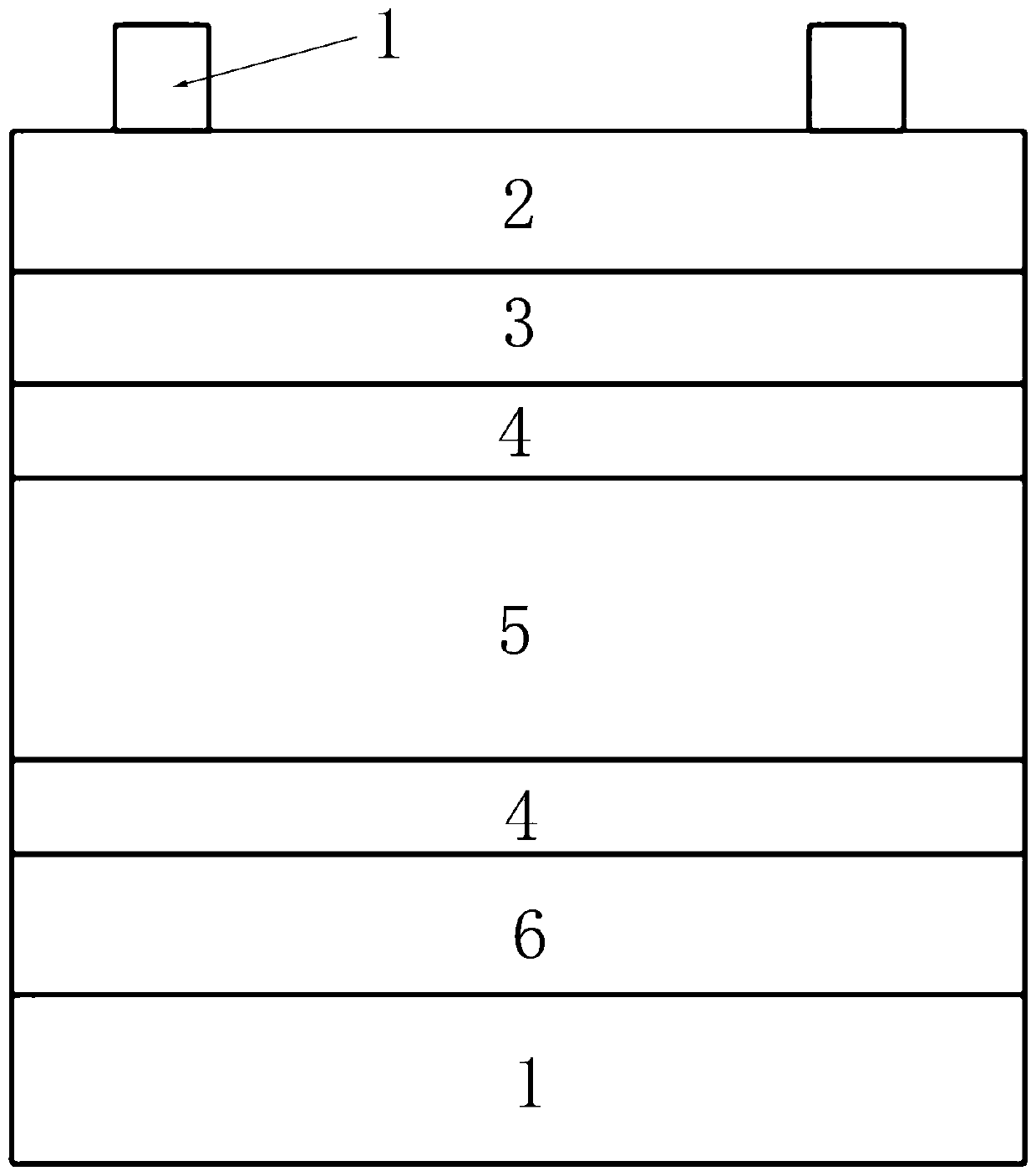
[0028] See attached picture. The battery described in this embodiment has the following structure from top to bottom: Ag electrode 1, ITO thin film 2 (70nm), NiOx:Mg thin film 3 (10nm), SiOx layer 4 (1.4nm), n-c-Si layer 5 , SiOx layer 4 (1.4nm), TiOx thin film 6 (10nm), Ag electrode 1.

[0029] When preparing:

[0030] 1. Wafer cleaning

[0031] The oxide-passivated non-doped crystalline silicon solar cell designed in this embodiment, in order to reduce the impurity concentration on the surface of the silicon wafer and reduce the interface defect state density between the surface of the silicon wafer and the passivation layer, therefore clean the surface of the silicon wafer The requirements are very high, and the cleaning of the silicon wafer is also critical to the subsequent growth of ultra-thin silicon oxide.

[0032] The silicon wafer used in the experiment is an n-type double-sided polished Czochralski single crystal silicon wafer with a thickness of 180-220 μm and a r...


PUM

PropertyMeasurementUnit
electrical resistivityaaaaaaaaaa
thicknessaaaaaaaaaa
electrical resistivityaaaaaaaaaa

Abstract

The invention discloses an oxide passivation contact solar cell and a preparation method thereof. The cell has the following structure from top to bottom: Ag / ITO / NiOx:Mg / SiOx / n-c-Si / SiOx / TiOx / Ag. Thepreparation method comprises the following steps of putting a cleaned silicon wafer into a HNO3 solution for thermal oxidation growth, growing a magnesium-doped nickel oxide thin film by utilizing a magnetron sputtering method, and growing a titanium oxide thin film by a magnetron sputtering method; dividing the silicon wafer into a sample with the area of 1.5*1.5cm2 by utilizing a laser scribingtechnology, and then growing an ITO transparent conductive thin film and a metal silver electrode by a magnetron sputtering method; and naturally cooling the manufactured cell to room temperature after annealing. The method does not need expensive thin film deposition equipment such as plasma chemical vapor deposition (PECVD) or atomic layer deposition (ALD), and has the characteristics of simpleprocess, low cost, environmental friendliness and the like.

Description

technical field [0001] The invention belongs to the technical field of solar cells, in particular to a solar cell with an oxide passivation contact and a preparation method thereof. Background technique [0002] At present, the mainstream product in the photovoltaic market is crystalline silicon solar cells. Its working principle is to use doping to form a p-n junction in the silicon wafer. Due to the built-in electric field in the p-n junction, the photogenerated carriers (electron-hole pairs) generated by light Separation under the action of the built-in electric field, electrons move toward the n-region, holes move toward the p-region, and are finally collected by two electrodes on the surface of the silicon wafer. Silicon wafer doping process The key process of crystalline silicon cells is generally carried out at high temperature (800-1000°C). After doping, it is necessary to remove the silicon wafer surface diffused at high temperature to form phosphosilicate glass or ...

Claims


Application Information

Patent Timeline
Patent Type & Authority Applications(China)
IPC IPC(8): H01L31/0216H01L31/18
CPCH01L31/02167H01L31/1868Y02E10/50Y02P70/50
Inventor 黄仕华张嘉华金日升
Owner ZHEJIANG NORMAL UNIVERSITY
Why Eureka
Try Eureka