
Method for reducing lateral erosion amount of copper microelectrode of piezoelectric ink-jet printing head by adopting multi-step corrosion
An inkjet printing head and micro-electrode technology, which is applied in the process of producing decorative surface effects, printing, microstructure technology, etc., can solve the problems of large side erosion during the residence time, residual positive glue structure, and difficult removal, etc. Achieve the effect of good corrosion uniformity, simple process and good repeatability
Patent Information
- Authority / Receiving Office
- CN · China
- Patent Type
- Applications(China)
- Current Assignee / Owner
- Publication Date
- 2019-12-03
Smart Images
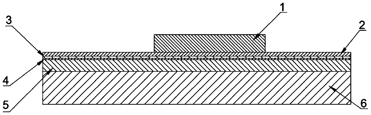
Figure 1 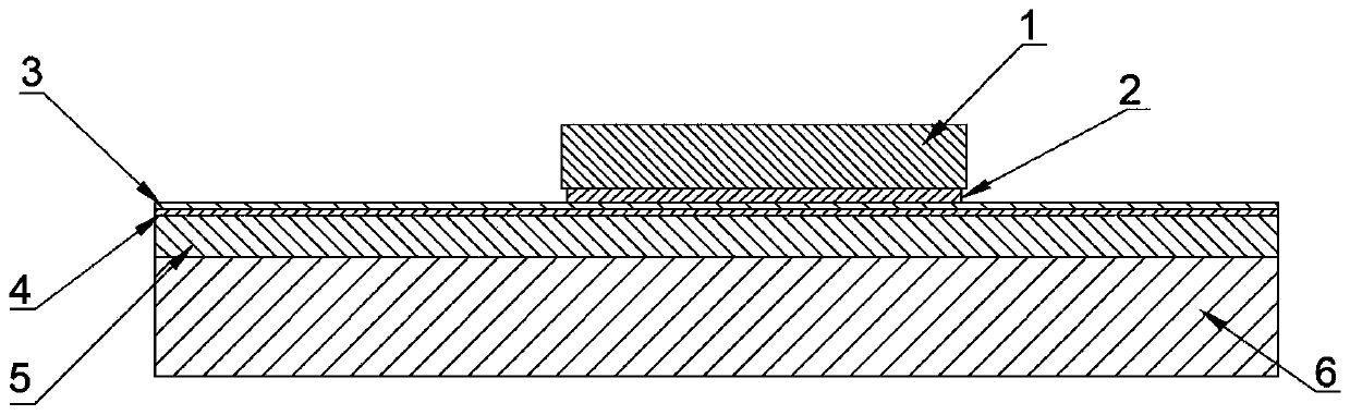
Figure 2 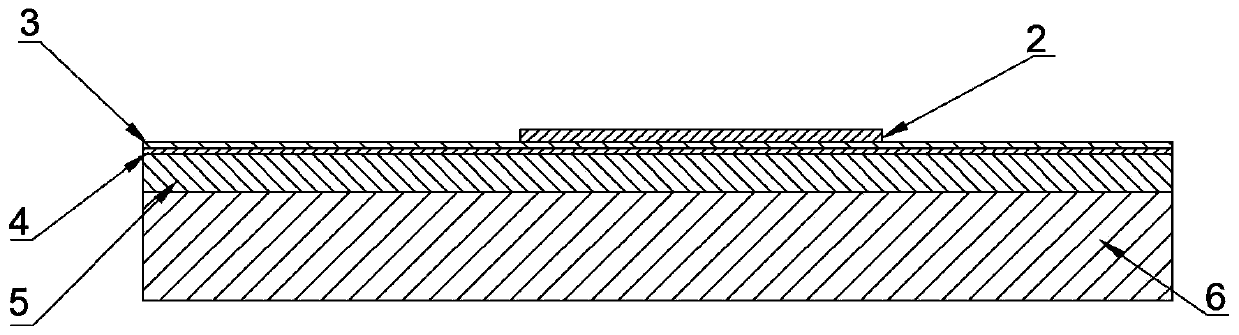
Figure 3
Abstract
Description
technical field
[0001] The invention belongs to the technical field of metal microelectrode preparation in the field of MEMS, and in particular relates to a method for reducing the amount of side erosion of a copper microelectrode of a piezoelectric inkjet printing head by using multi-step corrosion. Background technique
[0002] Piezoelectric inkjet printing technology has been expanded from the traditional printing industry to the fields of electronics, biology and rapid prototyping technology due to its advantages of miniaturization, mass production and long life; as the driving element of piezoelectric inkjet printing head, electrodes Material selection, manufacturing quality, and patterning process have a great influence on the vibration amplitude and vibration shape of the overall device. Metal Cu has been widely used in the field of microelectronic devices due to its excellent electrical conductivity, thermal conductivity and elasticity, and it is mostly used in the f...
Examples
Embodiment 1
[0028] (1) The piezoelectric inkjet printing head copper microelectrode film 2 was prepared by magnetron sputtering. First put the print head substrate 6 of the existing PZT substrate 5 on the hot plate before drying at 150°C to remove moisture, put it in the sputtering apparatus and evacuate it to 3.0×10 -5 Pass into the inert gas Ar after Pa; After the vacuum degree reaches 1.5Pa, sputter the Cr film 4 of 80nm and the Au film 3 of 200nm on the PZT substrate 5 successively, for increasing the binding force of the copper microelectrode film 2 and the PZT substrate 5 ; Then sputter the copper microelectrode film 2 of 600nm.
[0029] (2) Spin-coat one deck BP212 photoresist masking layer 1 on the copper microelectrode film base 2 of the piezoelectric inkjet printing head, the spin-coating speed of BP212 photoresist masking layer 1 is 600rpm at a low speed, and bake before the hot plate The temperature is 85 degrees, the time is 30min, and the exposure intensity is 3mW / cm 2 , t...
Embodiment 2
[0033] (1) The piezoelectric inkjet printing head copper microelectrode film 2 was prepared by magnetron sputtering. First put the print head substrate 6 with the existing PZT substrate 5 on the hot plate before drying at 150°C to remove moisture, put it in the sputtering apparatus and evacuate it to 3.0×10 -5 Pass into the inert gas Ar after Pa; After the vacuum degree reaches 1.5Pa, sputter the Cr film 4 of 80nm and the Au film 3 of 200nm on the PZT substrate 5 successively, for increasing the binding force of the copper microelectrode film 2 and the PZT substrate 5 ; Then sputter the copper microelectrode film 2 of 600nm.
[0034] (2) Spin-coat one deck BP212 photoresist masking layer 1 on the copper microelectrode film substrate 2 of the piezoelectric inkjet printing head, the spin-coating speed of BP212 photoresist masking layer 1 is a high speed 2200rpm, and bake before the hot plate The temperature is 90 degrees, the time is 20min, and the exposure intensity is 4mW / cm ...
Embodiment 3
[0041] (1) A piezoelectric inkjet printhead copper microelectrode film 2 was prepared by using a magnetron sputtering apparatus, which was consistent with the method in Example 2, and finally a 500 nm copper microelectrode film 2 was obtained by sputtering.
[0042] (2) Spin-coat one deck BP212 photoresist masking layer 1 on the copper microelectrode film substrate 2 of the piezoelectric inkjet printing head, the spin-coating speed of BP212 photoresist masking layer 1 is 1400rpm, and the baking temperature before the hot plate The temperature is 80 degrees, the time is 25min, and the exposure intensity is 3.2mW / cm 2 , the exposure time is 95s, the NaOH solution with a mass fraction of 0.3% is used for development for 35s, and the film is hardened with a hot plate at 80°C for 25min to obtain a pattern of the masking layer.
[0043] (3) the copper film electrode piece that step (2) obtains with BP212 photoresist masking layer 1 and copper microelectrode film 2 is placed in FeCl ...