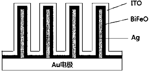
Preparation method of bismuth ferrite nanowire solar cell
A solar cell, bismuth ferrite nanotechnology, applied in nanotechnology, nanotechnology, nanotechnology for information processing, etc., can solve the problems of low photocurrent density and low photoelectric conversion efficiency of BiFeO3 materials
- Summary
- Abstract
- Description
- Claims
- Application Information
AI Technical Summary
Problems solved by technology
Method used
Image

Examples
specific Embodiment 1
[0028] 1. High-purity Al sheet annealing
[0029] The annealing temperature is 500°C, the annealing time is 4 hours, and it is taken out after being cooled to room temperature with the furnace.
[0030] 2. ultrasonic cleaning
[0031] Sonicate with acetone, ethanol, and deionized water for 3 minutes in sequence to remove stains on the surface of the Al sheet.
[0032] 3. remove natural oxide layer
[0033] Use 2 mol / L NaOH solution, the temperature is 60 ℃, the soaking time is 2 minutes, then take it out and rinse it with deionized water to remove the natural oxide layer.
[0034] 4. electrochemical polishing
[0035] Put the Al sheet into a mixed solution of 5vol% sulfuric acid, 95vol% phosphoric acid and 20 g / L chromic acid, use a stirring device to circulate and stir the mixed solution, perform electrochemical polishing for 5 minutes, the temperature of the water bath is 85 °C, and the polishing current is 0.8 A, then take it out and clean it with deionized water. ...
specific Embodiment 2
[0055] The difference between this embodiment and the specific example 1 is that in step 5, the voltage of anodic oxidation is changed to 10 V, 25 V, 60 V, and 100 V respectively, and then the pore sizes are respectively 20 nm, 35 nm, 80 nm, and 120 nm. nm porous alumina template, other steps and parameters are the same as those in Embodiment 1.
[0056] Implementation effect: the optical bandgap of BiFeO3 nanowires is 2.4 eV, under the irradiation of AM 1.5, 100 mW / cm2 standard light intensity, the short-circuit current density is 6-8 mA / cm2, the open-circuit voltage is 0.8-1 V, the efficiency It is 0.8-1.2%.
specific Embodiment 3
[0058] The difference between this embodiment and the specific example 1 is that in step 7, the double-pass porous alumina template is immersed in 6wt% phosphoric acid to expand the pores for 5-40 minutes, and a double-pass alumina template with a pore size of 60-200 nm can be obtained. Other steps and parameters are the same as those in the first embodiment.
[0059] Implementation effect: the optical bandgap of BiFeO3 nanowires is 2.4 eV, under the irradiation of AM 1.5, 100 mW / cm2 standard light intensity, the short-circuit current density is 6-7 mA / cm2, the open-circuit voltage is 0.8-0.9 V, the efficiency It is 0.8-1%.
PUM
| Property | Measurement | Unit |
|---|---|---|
| Thickness | aaaaa | aaaaa |
| Thickness | aaaaa | aaaaa |
| Aperture | aaaaa | aaaaa |
Abstract
Description
Claims
Application Information