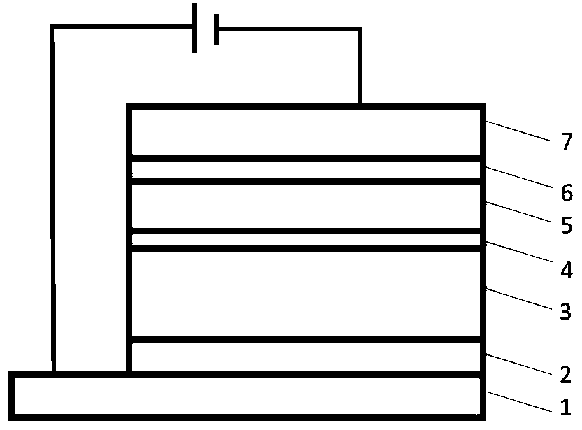
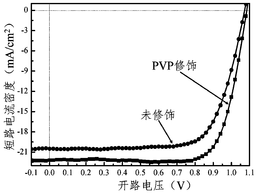
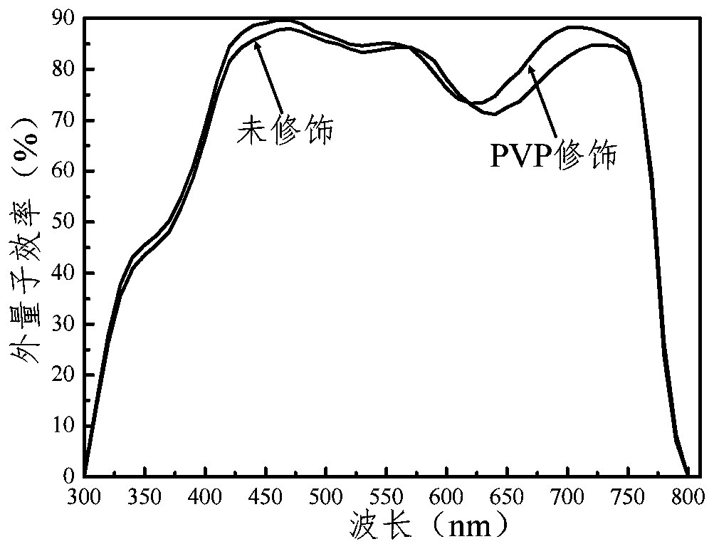
Inverted planar heterojunction hybrid perovskite solar cell and preparation method thereof
A solar cell and perovskite technology, applied in circuits, photovoltaic power generation, electrical components, etc., can solve the problems of reducing defect state density and increasing energy loss, and achieve the effect of good light absorption characteristics
- Summary
- Abstract
- Description
- Claims
- Application Information
AI Technical Summary
Problems solved by technology
Method used
Image
Examples
Embodiment 1
[0035] 1) Clean the patterned silver nanowire flexible substrate with acetone, cleaning solution, deionized water three times and isopropanol in sequence for 15-30 minutes respectively. After ozone treatment for 15 to 30 minutes, put it into a nitrogen-protected glove box for subsequent use;
[0036] 2) MoO x Deposited on the flexible substrate of nano-silver wire as a hole transport layer by spin coating method, the film thickness is about 5-20 nanometers, and annealed on a hot stage at 80-100°C for 15-30 minutes;
[0037] 3) 1.2-1.3mol / L of PbI 2 :MAI (1.2:0.3) mixed solution is spin-coated on the MoOx film layer with the speed of 6Krpm, and during the spin-coating process, the MAI solution of 40mg / ml is drip-coated from top to bottom. Then the film is placed on a hot stage at 90-110° C., and annealed for 15-30 minutes. where PbI 2 : the solvent of the MAI mixed solution is DMF, and the MAI solution is dissolved in Virahol;
[0038] 4) Spin-coat PVP dissolved in isoprop...
Embodiment 2
[0043] 1) Clean the patterned copper nanowire substrate with acetone, cleaning solution, deionized water three times and isopropanol in sequence for 15-30 minutes respectively. After processing for 15-30 minutes, put it into a nitrogen-protected glove box for standby;
[0044] 2) NiO x Deposited on the copper nanowire substrate as a hole transport layer by spin coating method, the film thickness is about 5-20 nm, and annealed on a hot stage at 80-100°C for 15-30 minutes;
[0045] 3) 1.2-1.3mol / L of PbI 2 :MAI (1:1) mixed solution was spin-coated on NiO at a speed of 4Krpm x On the film layer, during the spin coating process, chlorobenzene was drop-coated from top to bottom. Then the film is placed on a hot stage at 90-110° C., and annealed for 15-20 minutes. where PbI 2 : The solvent of the MAI mixed solution is DMF;
[0046] 4) Spin-coat PVP dissolved in isopropanol on the perovskite film with a thickness of 1-8 nanometers, and anneal on a hot stage at 50-120° C. for 10...
Embodiment 3
[0051] 1) Clean the patterned FTO glass substrate with acetone, cleaning solution, three times of deionized water and isopropanol for 15-30 minutes respectively. After cleaning, dry it with nitrogen and put it into a petri dish, and treat it with ultraviolet ozone. After 15 to 30 minutes, put it into a nitrogen-protected glove box for standby;
[0052] 2) Deposit PEDOT:PSS on the FTO glass substrate by spin coating method as a hole transport layer, the film thickness is about 5-20 nm, and anneal on a hot stage at 80-100°C for 15-30 minutes;
[0053] 3) 368.8mg PbI 2 and 55.634 mg PbCl 2 Dissolved together in 1ml DMF to form a precursor solution, spin-coated on the PEDOT:PSS film layer at a speed of 6Krpm, during the spin-coating process, drop-coated 70mg / ml MAI solution from top to bottom. Then the film is placed on a hot stage at 90-110° C., and annealed for 15-20 minutes. Wherein the solvent of the MAI mixed solution is Virahol;
[0054] 4) Spin-coat PVP dissolved in iso...
PUM
| Property | Measurement | Unit |
|---|---|---|
| Thickness | aaaaa | aaaaa |
| Thickness | aaaaa | aaaaa |
| Thickness | aaaaa | aaaaa |
Abstract
Description
Claims
Application Information


