
Preparation method of silicon dioxide nanorod array

A nanorod array and silicon dioxide technology, applied in the field of nanomaterials, can solve the problems of complex step-by-step operations, expensive reaction equipment, harsh reaction conditions, etc., and achieve simple and efficient preparation process, low equipment operation requirements, and no pollution in the preparation process Effect

Active Publication Date: 2020-05-12
SUZHOU UNIV
View PDF6 Cites 3 Cited by
  • Summary
  • Abstract
  • Description
  • Claims
  • Application Information

AI Technical Summary

Problems solved by technology

However, these nanorod array structures are all based on the growth mechanism of VLS, and this growth mechanism is usually accompanied by problems such as high energy consumption, expensive reaction equipment, harsh reaction conditions, etc., and usually requires gold as a catalyst, which is expensive
[0004] Furthermore, most other existing methods for preparing nanorod array structures involve multiple steps, and they are generally complex in step-by-step operations, making it difficult to scale up production and practical applications.

Method used


Image

  • Preparation method of silicon dioxide nanorod array
  • Preparation method of silicon dioxide nanorod array
  • Preparation method of silicon dioxide nanorod array

Examples


preparation example Construction

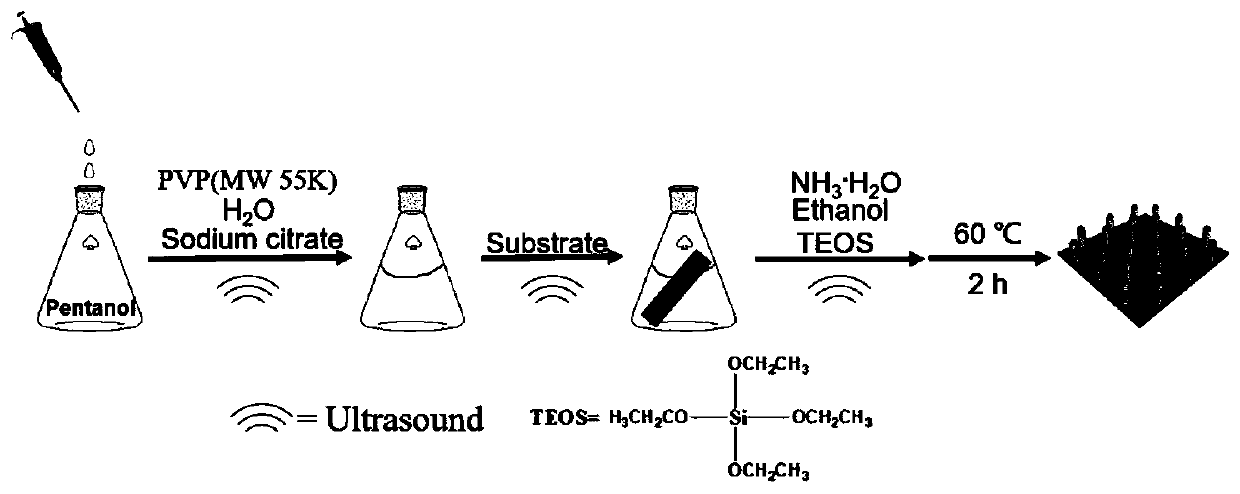
[0024] The invention provides a method for preparing a silica nanorod array, comprising: mixing an organic surfactant solution with a sodium citrate aqueous solution, then putting it into a hydrophilic substrate, adding a basic catalyst, and after ultrasonic treatment, adding The silicon source is left to stand, and the substrate is taken out to obtain a silicon dioxide nanorod array.

[0025] see figure 1 , figure 1 Schematic diagram of the preparation process of the silica nanorod array provided by the present invention.

[0026] Among them, the present invention has no special limitation on the sources of all raw materials, which can be commercially available.

[0027] The surfactant organic solution is mixed with the sodium citrate aqueous solution; The surfactant in the described surfactant organic solution is preferably polyvinylpyrrolidone (PVP), cetyltrimethylammonium bromide (CTAB), lauryl One or more of sodium alkyl sulfate (SDS) and polyacrylic acid (PAA), more p...

Embodiment 1

[0040] 1.1 Cleaning of the substrate: First, ultrasonically clean the ITO glass substrate with acetone, deionized water and absolute ethanol, and dry the substrate with nitrogen gas for later use.

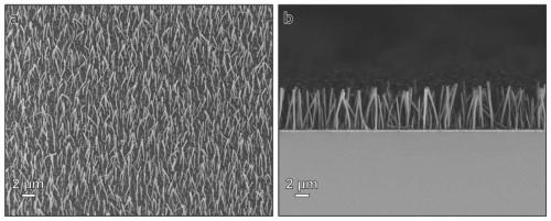
[0041] 1.2 Synthesis of silica nanorod arrays: 1 g of PVP (MW 55000) was dissolved in 10 mL of 1-pentanol by sonication, and 380 μL of aqueous sodium citrate (0.053 M) was added. Then the cleaned ITO substrate was immersed in the above solution. Then 200 μL of ammonium hydroxide solution (concentration 25%-28%) and 1 mL of ethanol were added to the reaction. Vigorous stirring was provided by ultrasonic treatment (power 60%, time 10 seconds, water temperature 20° C.) to form a stable emulsion system. The growth of silica nanorods starts with the addition of 100 μL of tetraethyl silicate (after adding tetraethyl silicate, it needs to be treated with 60% ultrasonic power for 10 seconds before standing still). The mixed solution was left to stand at 60° C. for 4 hours. Finally, the ...

Embodiment 2

[0044] 2.1 Cleaning of the substrate: Ultrasonic cleaning of the ITO glass substrate was performed with acetone, deionized water and absolute ethanol, and the substrate was blown dry with nitrogen gas for later use.

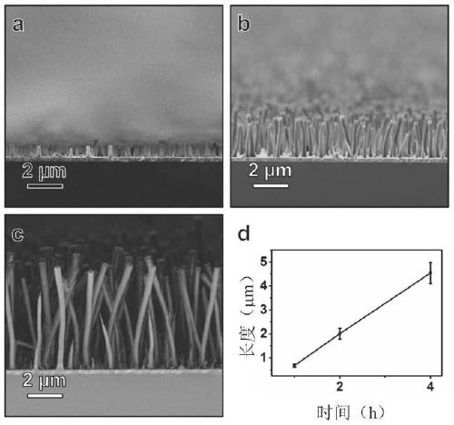
[0045] 2.2 Synthesis of silica nanorod arrays: In a typical experiment, 1 g of PVP (MW55000) was dissolved in 10 mL of 1-pentanol by sonication, and 380 μL of aqueous sodium citrate (0.053 M) was added. The cleaned substrate is then immersed in the above solution. Then 200 μL of ammonium hydroxide solution (concentration 25%) and 1 mL of ethanol were added to the reaction. Vigorous stirring was provided by ultrasonic treatment (power 99%, time 20 seconds, water temperature 30° C.) to form a stable emulsion system. The growth of silica nanorods starts with the addition of 100 μL of tetraethyl silicate (sonication first and then resting, ultrasonic power 99% for 20 seconds and then resting). The mixed solutions were left standing at 60°C for 1 hour, 2 hours and 4...


PUM

PropertyMeasurementUnit
diameteraaaaaaaaaa
lengthaaaaaaaaaa
lengthaaaaaaaaaa

Abstract

The invention provides a preparation method of a silicon dioxide nanorod array, comprising the following steps: mixing a surfactant organic solution with a sodium citrate aqueous solution, putting into a hydrophilic substrate, adding a basic catalyst, carrying out ultrasonic treatment, adding a silicon source, standing, and taking out the substrate to obtain the silicon dioxide nanorod array. Compared with the prior art, the invention has the following beneficial effects: with the utilization of the solubility difference of water-soluble salt in an organic solvent-water mixed solution, salt liquid drops are separated out and adsorbed on the hydrophilic substrate, the silicon source is subjected to catalytic hydrolysis by using an alkaline catalyst in the liquid drops to prepare the silicondioxide nano array on the substrate, and then seed-free one-step growth is achieved through a solution liquid-phase solid-phase growth mechanism; the used raw materials are cheap and free of pollution, the preparation process is simple and efficient, no pollutant is generated, energy consumption is low, the requirement for equipment operation is low, mass production is easy to expand, and the diameter and length of the silicon dioxide nanorods can be adjusted through the standing temperature and time.

Description

technical field [0001] The invention belongs to the technical field of nanometer materials, in particular to a method for preparing a silicon dioxide nanorod array. Background technique [0002] One-dimensional nanorod arrays have unique physical properties and geometric structures, such as short electron diffusion distances, allowing integration into more complex structures, providing sufficient space for material diffusion and light harvesting capabilities, etc., in photocatalysis, electrocatalysis, biochemical sensors The field of energy storage and conversion has attracted more and more attention. [0003] In the past few decades, the vapor-liquid-solid (VLS) mechanism has been extensively studied as it provides an effective way to fabricate 1D nanorod arrays. For example, Wang et al. reported the growth of ZnO onto single-crystal alumina substrates based on a self-assembled template, which was subsequently used in piezoelectric nanogenerators (Wang, Z.L.; Song, J., Pie...

Claims


Application Information

Patent Timeline
Patent Type & Authority Applications(China)
IPC IPC(8): C01B33/12C03C17/25
CPCC01B33/12C03C17/25C01P2004/10C01P2004/62C01P2004/03C03C2217/213C03C2218/111Y02E10/542
Inventor 何乐李超然方耀思
Owner SUZHOU UNIV
Learn More