Perovskite photoelectric detector based on hole transport layer and preparation method thereof

A technology of hole transport layer and photodetector, which is applied in photovoltaic power generation, electric solid-state devices, semiconductor/solid-state device manufacturing, etc., can solve the problems of Spiro-OMeTAD low mobility, short life, poor device stability, etc., and achieve high Air stability and isolation of water and oxygen, improved stability and life, and low cost

Inactive Publication Date: 2020-07-17
UNIV OF ELECTRONICS SCI & TECH OF CHINA
View PDF7 Cites 0 Cited by
  • Summary
  • Abstract
  • Description
  • Claims
  • Application Information

AI Technical Summary

Problems solved by technology

[0005] The object of the present invention is: in order to solve the technical problems of the traditional hole transport layer material Spiro-OMeTAD low mobility, poor device stability and short life, the invention provides a perovskite photodetector based on the hole transport layer and its preparation method

Method used


Image

  • Perovskite photoelectric detector based on hole transport layer and preparation method thereof
  • Perovskite photoelectric detector based on hole transport layer and preparation method thereof
  • Perovskite photoelectric detector based on hole transport layer and preparation method thereof

Examples


Embodiment 1

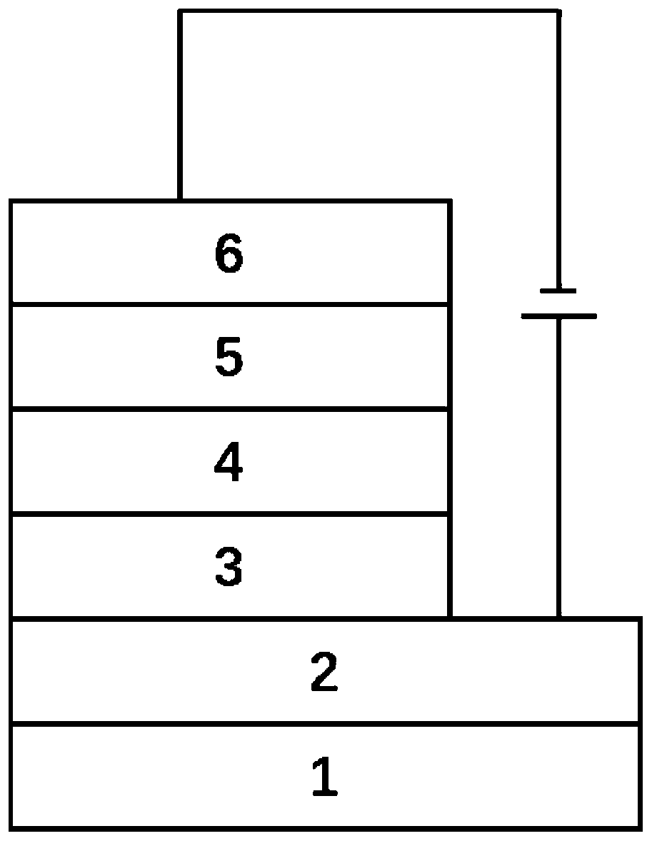
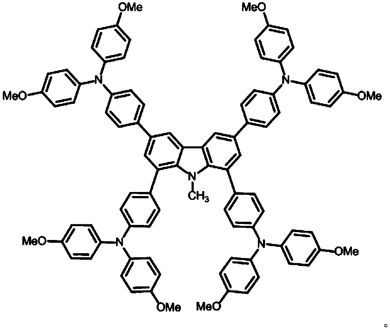
[0048] The substrate composed of the substrate and the transparent conductive anode ITO is cleaned, and dried with nitrogen after cleaning; the surface of the transparent conductive anode ITO is spin-coated with SnO2 (water dispersion, the spin-coating speed is 3000rpm, the spin-coating time is 30s, the thickness 20-30nm) to prepare an electron transport layer, and thermally anneal the formed film (annealing temperature 150°C, annealing time 15min); spin-coat the MAPbI3 precursor solution on the electron transport layer (mixed with DMF as a solvent to form a solute concentration For the mixed solution of 500mg / mL, the spin-coating speed is 4000rpm, the spin-coating time is 30s, and the thickness is 500nm) to prepare the perovskite photoactive layer. Inhibit the disordered crystallization of perovskite, and then anneal at 120°C for 20min; spin-coat Car-4-TPA solution (dissolved in chlorobenzene solution at a concentration of 50mg / ml, without any doping) to prepare the hole tran...

Embodiment 2

[0051] The substrate composed of the substrate and the transparent conductive anode ITO is cleaned, and dried with nitrogen after cleaning; the surface of the transparent conductive anode ITO is spin-coated with SnO2 (water dispersion, the spin-coating speed is 3000rpm, the spin-coating time is 30s, the thickness 20-30nm) to prepare an electron transport layer, and thermally anneal the formed film (annealing temperature 150°C, annealing time 15min); spin-coat the MAPbI3 precursor solution on the electron transport layer (mixed with DMF as a solvent to form a solute concentration For the mixed solution of 500mg / mL, the spin-coating speed is 4000rpm, the spin-coating time is 30s, and the thickness is 500nm) to prepare the perovskite photoactive layer. Inhibit the disordered crystallization of perovskite, and then anneal at 120°C for 20 minutes; spin-coat Car-4-TPA solution (dissolved in chlorobenzene solution at a concentration of 50mg / ml, and mix with Li-TFSI) was used to prepa...

Embodiment 3

[0054] The substrate composed of the substrate and the transparent conductive anode ITO is cleaned, and dried with nitrogen after cleaning; the surface of the transparent conductive anode ITO is spin-coated with SnO2 (water dispersion, the spin-coating speed is 3000rpm, the spin-coating time is 30s, the thickness 20-30nm) to prepare an electron transport layer, and thermally anneal the formed film (annealing temperature 150°C, annealing time 15min); spin-coat the MAPbI3 precursor solution on the electron transport layer (mixed with DMF as a solvent to form a solute concentration For the mixed solution of 500mg / mL, the spin-coating speed is 4000rpm, the spin-coating time is 30s, and the thickness is 500nm) to prepare the perovskite photoactive layer. Inhibit the disordered crystallization of perovskite, and then anneal at 120°C for 20min; spin-coat DNT-4TPA solution (dissolved in chlorobenzene solution at a concentration of 50mg / ml, and doped with Li -TFSI and FK209) to prepare...


PUM

PropertyMeasurementUnit
thicknessaaaaaaaaaa
thicknessaaaaaaaaaa
thicknessaaaaaaaaaa

Abstract

The invention discloses a perovskite photoelectric detector based on a hole transport layer and a preparation method thereof, and relates to the technical field of photoelectric detectors. The perovskite photoelectric detector comprises a transparent substrate, a conductive anode, an electron transport layer, a perovskite photoactive layer, a hole transport layer and a metal cathode which are sequentially arranged from bottom to top, and the perovskite hole transport layer is made of Car-4-TPA, is simple in molecular structure, high in hole mobility, high in conductivity, good in solubility and higher in energy level. The reverse injection of the perovskite photoelectric detector prepared from the hole transport material is little, a dark-state current of the perovskite photoelectric detector is effectively improved, and meanwhile, a photocurrent of the perovskite photoelectric detector can be improved, so that the detection rate of the device is improved. Compared with the Spiro-OMeTAD used by a traditional device, the hole transport layer does not need to be oxidized, and the erosion of water and oxygen to the device can be effectively reduced, and therefore the stability of theperovskite photoelectric detector is improved, and the service life of the perovskite photoelectric detector is prolonged.

Description

technical field [0001] The invention relates to the technical field of photodetection devices, in particular to a perovskite photodetector based on a hole transport layer and a preparation method thereof. Background technique [0002] With the development of human society, mankind has entered the information age. While the Internet brings society into intelligence, automation and high speed, it also improves the efficiency, integration, multi-function, energy saving and miniaturization of various equipment. Higher requirements have been put forward in terms of globalization and environmental protection. Since it is difficult for traditional electronic equipment to meet the requirements of so many indicators at the same time, a large number of emerging multi-functional, integrated and intelligent integrated equipment have emerged as the times require. Among them, photodetectors can be used in machine vision, aerospace technology, missile tail flame warning, space detection t...

Claims


Application Information

Patent Timeline
Patent Type & Authority Applications(China)
IPC IPC(8): H01L51/42H01L51/46H01L51/48
CPCH10K85/624H10K85/6572H10K85/30H10K30/15Y02E10/549
Inventor 于军胜郑丁钟建李嘉文
Owner UNIV OF ELECTRONICS SCI & TECH OF CHINA
Why Eureka
Try Eureka