SBD device structure and preparation method thereof

A device structure and epitaxial layer technology, which is applied in semiconductor/solid-state device manufacturing, semiconductor devices, electrical components, etc., can solve the problems of small saturation current, high switching loss, and large turn-on voltage, so as to improve saturation current and breakdown performance, the effect of reducing the turn-on voltage

Active Publication Date: 2020-10-16
CHANGCHUN INST OF OPTICS FINE MECHANICS & PHYSICS CHINESE ACAD OF SCI
View PDF9 Cites 2 Cited by
  • Summary
  • Abstract
  • Description
  • Claims
  • Application Information

AI Technical Summary

Problems solved by technology

However, there are still some problems that need to be solved urgently in the existing GaN SBD: (1) when the GaN SBD is turned on, the on-resista

Method used


Image

  • SBD device structure and preparation method thereof
  • SBD device structure and preparation method thereof

Examples


preparation example Construction

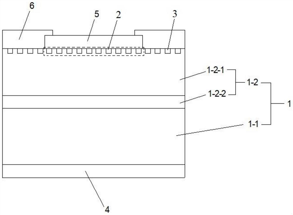
[0070] The preparation method of the floating metal ring 3 is as follows: a floating metal ring accommodation groove is etched on the epitaxial layer 1-2, and the floating metal ring 3 is deposited in the floating metal ring accommodation groove, so as to ensure that the floating metal ring 3 and the epitaxial layer 1-2 flush. For example: the ring width of the floating metal ring 3 is 3-5 μm, and the ring spacing is 3-5 μm.

[0071] In another specific embodiment of the present invention, an insulating layer 6 is grown on the epitaxial layer 1-2 corresponding to the floating metal ring 3, and the material of the insulating layer 6 is silicon nitride, silicon dioxide or aluminum oxide .

[0072] The insulating layer 6 effectively suppresses the electric field breakdown at the edge of the Schottky contact electrode 5 and the surface of the device, increases the reverse breakdown voltage, and effectively improves the performance of the SBD device.

[0073] The above describes ...

Embodiment 1

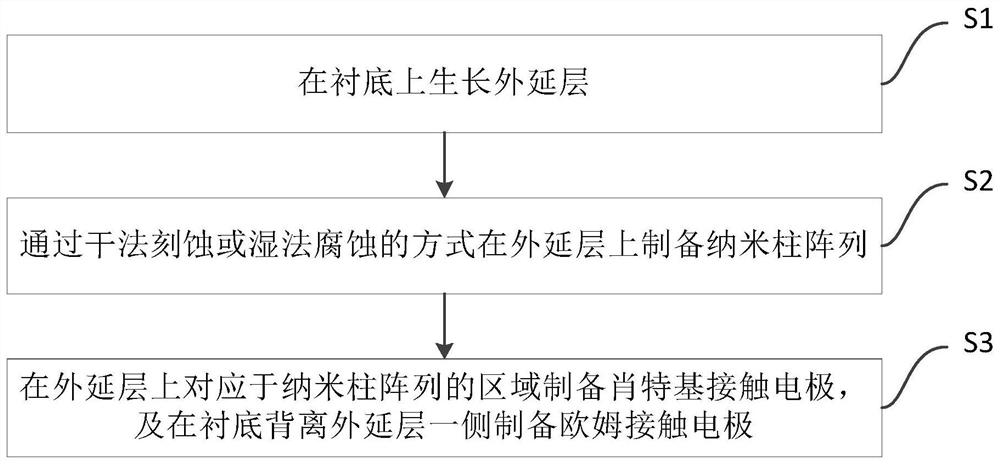
[0125] A double-sided polished n-type highly doped self-supporting gallium nitride substrate was selected as the substrate, and organic chemical vapor deposition (MOCVD) was used to sequentially grow the gallium nitride substrate with a thickness of 2 μm and a carrier concentration of 1.5× 10 18 cm -3 the n + type gallium nitride and the thickness is about 23μm, the carrier concentration is about 8×10 15 cm -3 n-type gallium nitride. Hydrogen silanes can be used as Si raw materials for n-type dopants (donors).

[0126] The process parameters of the RTA process in the dry etching process are:

[0127] The annealing temperature is 800°C;

[0128] The annealing time was 60 seconds.


PUM

PropertyMeasurementUnit
Thicknessaaaaaaaaaa

Abstract

The invention provides an SBD device structure and a preparation method thereof. The SBD device structure comprises a substrate, an epitaxial layer grown on the substrate, a nanopillar array preparedin an accommodating groove in the epitaxial layer, a Schottky contact electrode prepared on the epitaxial layer and located in a nanopillar array region, and an ohmic contact electrode prepared on oneside, deviating from the epitaxial layer, of the substrate. According to the method, the Schottky contact area of the anode Schottky type metal-semiconductor of the SBD device is increased by utilizing the nanorods, and the forward conduction characteristic of the SBD device is comprehensively improved from two aspects: on one hand, the nanorods can increase the current density during conduction,so that the saturation current is increased, and the conduction resistance is reduced; and on the other hand, the nanopillar can enhance the control capability of the external bias voltage on the epitaxial layer, and the current driving capability of the SBD device is effectively improved, so that the turn-on voltage of the SBD device is reduced, and the switching loss is reduced.

Description

technical field [0001] The invention relates to the technical field of semiconductors, in particular to an SBD device structure based on a nanocolumn structure and a preparation method thereof. Background technique [0002] For a long time, mainstream power electronic devices on the market have been made based on silicon, but the performance of silicon-based devices has approached the limit of material theory and cannot meet the requirements of new applications. The third-generation semiconductor gallium nitride (GaN) with a band gap greater than 2.2eV has a large band gap, a strong critical breakdown electric field, a high saturation electron drift velocity, high thermal conductivity, high chemical stability, and strong radiation resistance. and other excellent material properties; therefore, GaN power electronic devices have high breakdown voltage, low on-resistance, and high switching frequency, and can be applied to more complex working environments such as high temperat...

Claims


Application Information

Patent Timeline
IPC IPC(8): H01L29/872H01L29/47H01L29/06H01L21/329
CPCH01L29/872H01L29/47H01L29/475H01L29/0611H01L29/66212
Inventor 黎大兵陈雨轩孙晓娟蒋科
Owner CHANGCHUN INST OF OPTICS FINE MECHANICS & PHYSICS CHINESE ACAD OF SCI
Why Eureka
Try Eureka