Room temperature wide spectrum photoelectric detector based on two-dimensional cobalt selenide thin film and preparation method

A technology of photodetector and cobalt selenide, which is applied in the field of photoelectric detection at room temperature, and can solve problems such as device instability and material oxidation

Active Publication Date: 2020-10-30
EAST CHINA NORMAL UNIVERSITY
View PDF0 Cites 1 Cited by
  • Summary
  • Abstract
  • Description
  • Claims
  • Application Information

AI Technical Summary

Problems solved by technology

In recent years, long-wave infrared photodetectors based on two-dimensional materials, such as black phosphorus-based photodetectors and black arsenic-phosphorus-based long-wave infrared photodetectors, have been discovered one after another. External factors such as the oxidation of such materials

Method used


Image

  • Room temperature wide spectrum photoelectric detector based on two-dimensional cobalt selenide thin film and preparation method
  • Room temperature wide spectrum photoelectric detector based on two-dimensional cobalt selenide thin film and preparation method
  • Room temperature wide spectrum photoelectric detector based on two-dimensional cobalt selenide thin film and preparation method

Examples


Embodiment 1

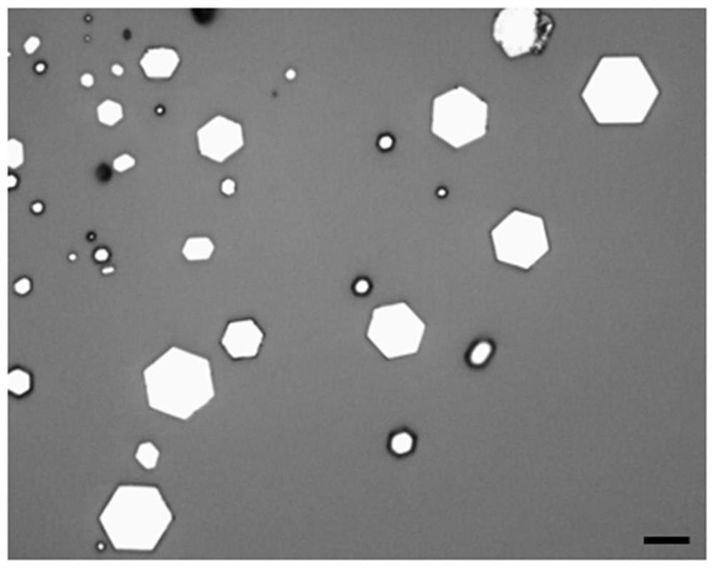
[0029] The chemical vapor deposition growth of two-dimensional cobalt selenide film on silicon dioxide-silicon substrate, the specific steps are:

[0030] 1. Substrate cleaning: use a 300nm silicon dioxide-silicon substrate as a growth substrate, place the substrate in an acetone solution with a concentration of 99.5%, and place it in isopropanol with a concentration of 99.5% after ultrasonic cleaning for 30 minutes solution, ultrasonic cleaning for 30 minutes and then placed in deionized water, ultrasonic cleaning for 30 minutes, it was taken out and dried with a nitrogen gun. A layer of 5nm cobalt film was plated on the cleaned substrate at a rate of 2.5nm / min by dual ion beam deposition. The steps are as follows: (1) stick the cleaned silicon dioxide-silicon substrate on On the metal sheet, open the air release valve, open the chamber, place the cobalt target and the metal sheet at the corresponding positions in the chamber, close the baffle and the chamber; (2) Close the a...

Embodiment 2

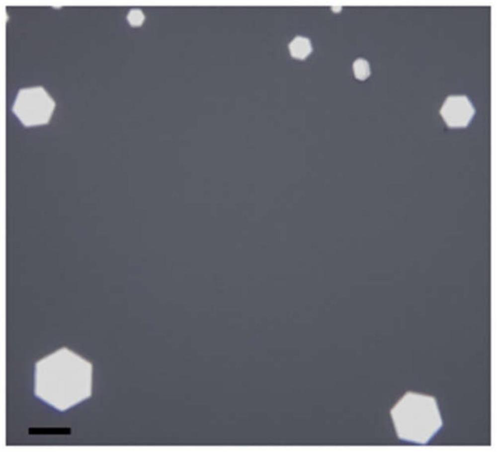
[0034] The chemical vapor deposition growth of two-dimensional cobalt selenide film on sapphire substrate, the specific steps are:

[0035] 1. Substrate cleaning: take the sapphire substrate as the growth substrate, place the substrate in an acetone solution with a concentration of 99.5%, ultrasonically clean it for 30 minutes, then place it in an isopropanol solution with a concentration of 99.5%, and ultrasonically clean it for 30 minutes. Then place it in deionized water, ultrasonically clean it for 30 minutes, take it out and dry it with a nitrogen gun. A layer of 3nm cobalt film was plated on the cleaned substrate at a rate of 2.5nm / min by dual ion beam deposition. The steps are as follows: (1) Stick the cleaned sapphire substrate on the metal sheet, Open the air valve, open the cavity, place the cobalt target and the metal sheet in the corresponding position in the cavity, close the baffle and the cavity; (2) close the purge valve, start the air pump, the upper pipe valv...

Embodiment 3

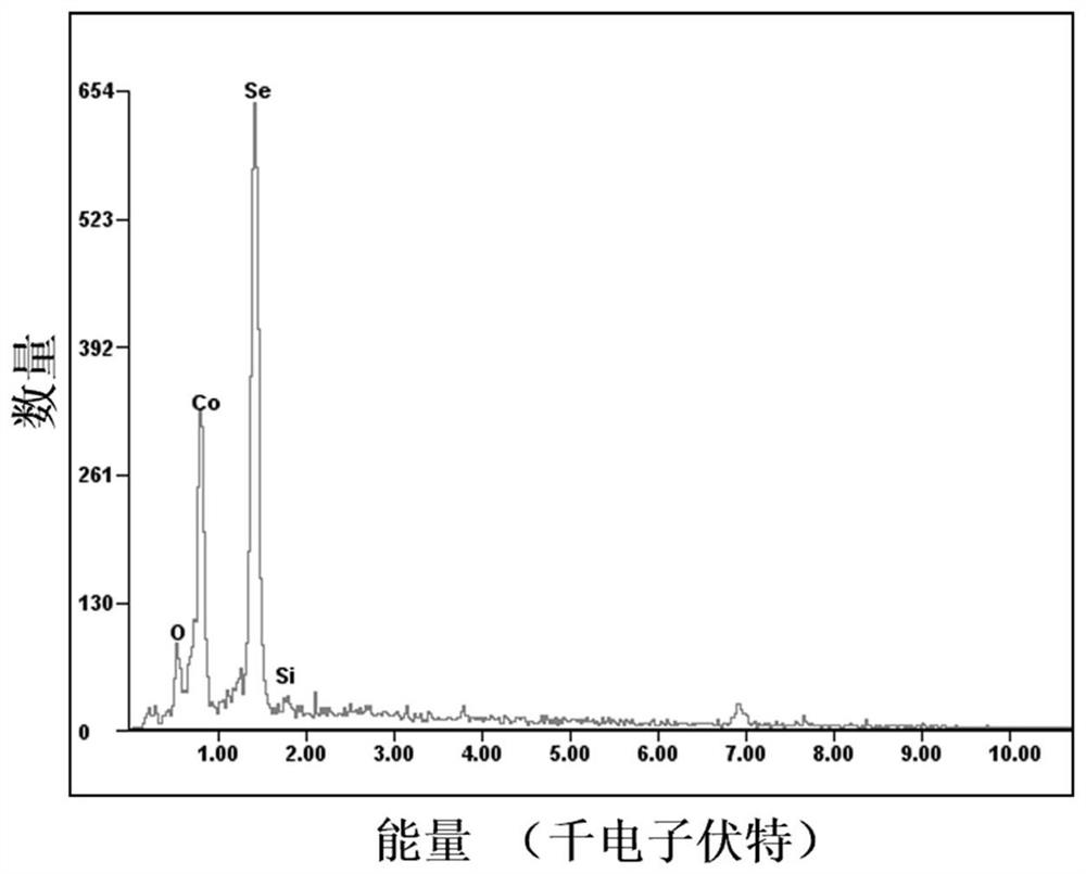
[0039] The preparation of a two-dimensional cobalt selenide film-based room temperature wide-spectrum photodetector, taking the two-dimensional cobalt selenide film prepared in Example 1 as an example, the specific steps are:

[0040] 1) Spin-coat polymethyl methacrylate on a silicon dioxide-silicon substrate with a cobalt selenide film using a spin coater at a speed of 4000 rpm and a spin coating time of 40 seconds;

[0041] 2) Place the cobalt selenide thin film substrate coated with polymethyl methacrylate on a heating table to cure for 5 minutes, and the curing temperature is 150 degrees Celsius;

[0042] 3) Electrodes are patterned on the cured cobalt selenide thin film substrate by electron beam exposure;

[0043] 4) Put the exposed sample into the developer solution for 10-30 seconds, then put the developed sample into isopropanol to remove the developer solution, then dry it with a nitrogen gun, and the electrode pattern can be observed under the microscope On cobalt ...


PUM


Abstract

The invention discloses a room temperature wide spectrum photoelectric detector based on a two-dimensional cobalt selenide thin film and a preparation method. A cobalt film with certain thickness is grown by sputtering on a substrate using dual-ion-beam sputtering technology; and on the basis, with cobalt selenide power and selenium powder being reaction source and argon as carrier gas, the cobaltselenide thin film is prepared using chemical vapor deposition method. Metal electrodes in ohmic contact with the cobalt selenide thin film are arranged on the cobalt selenide thin film as a source electrode and a drain electrode, and the photoelectric detector based on the two-dimensional cobalt selenide thin film is constituted. The obtained photoelectric detector based on the two-dimensional cobalt selenide thin film can realize an initial wide spectrum response waveband of 450 nanometer to 10.6 micrometer laser under room temperature, and the response rate reaches 2.58 watt / ampere. According to the provided room temperature wide spectrum photoelectric detector based on novel high-performance two-dimensional materials, the application of two-dimensional cobalt selenide materials is widened in the fields photoelectricity and magnetic-optical technology.

Description

technical field [0001] The invention relates to the field of photoelectric detection at room temperature, in particular to a two-dimensional cobalt selenide film-based room temperature wide-spectrum photodetector and a preparation method thereof. Background technique [0002] Photoelectric detectors have extensive and important applications in people's daily life, security, medicine, industry, climate monitoring, etc., especially in the field of aerospace, artificial earth satellite detection and infrared astronomical detection, as well as infrared warnings on high-end weapon platforms And guidance, infrared reconnaissance, infrared communication, etc., are the research hotspots that developed countries focus on and invest in, and are of great significance to the development of cutting-edge science and technology and the strengthening of the core forces of national defense. At present, my country's infrared detection technology is in the initial stage of development to the f...

Claims


Application Information

Patent Timeline
IPC IPC(8): C23C28/00C23C14/34C23C14/02C23C14/18C23C14/24C23C14/58C23C16/30H01L21/02H01L31/0272H01L31/18
CPCC23C28/322C23C28/34C23C14/3442C23C14/185C23C14/5866C23C14/021C23C16/305C23C14/24H01L21/02381H01L21/02568H01L21/0262H01L31/0272H01L31/18Y02P70/50
Inventor 吴幸梁芳王超伦
Owner EAST CHINA NORMAL UNIVERSITY
Why Eureka
Try Eureka