

Double-sided metal grid flexible conductive film and manufacturing method thereof
A flexible conductive, double-sided metal technology, used in cable/conductor manufacturing, conductive layers on insulating carriers, circuits, etc., can solve problems such as thick photoresist coating, reduced touch sensitivity, and large thickness of metal grids , to achieve the effect of clear and accurate circuit pattern, improved touch sensitivity, and easy flexible expression
- Summary
- Abstract
- Description
- Claims
- Application Information
AI Technical Summary
Problems solved by technology
Method used
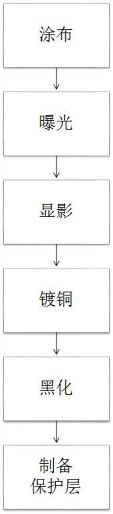
Image

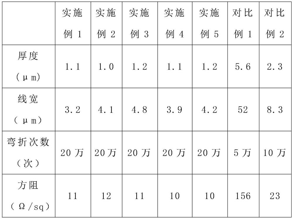
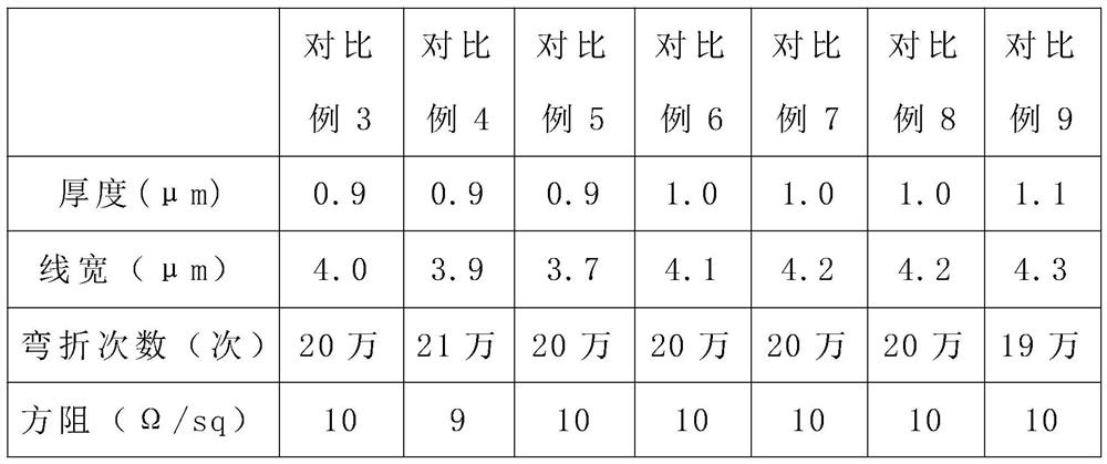
Examples
Embodiment 1
[0053] Take a flexible transparent substrate, apply photoresist on its upper surface and lower surface respectively, and then cure at 70°C for 10s to form a photoresist layer; then take 65% pure water, 5% palladium Catalyst, 5% solvent and 5% active agent are mixed and heated to 100 ° C, stirred for 1 hour to prepare a catalyst solution, take the catalyst solution to coat the surface of the photoresist layer, and dry to form a catalyst layer to prepare a base film A, wherein the base material is polyimide, the palladium catalyst is palladium oxide, the solvent is ethyl lactate, and the active agent is fluorosurfactant FC-4430;
[0054] Take the base film A, and irradiate its upper surface and lower surface with ultraviolet light, the wavelength of ultraviolet light is 314nm, and the exposure energy is 50mJ / cm 2 , at this time, the photoresist layer and the photoresist layer and the photoresist layer are cured in the light-receiving area, and the base film B is prepared;
[00...
Embodiment 2
[0060] Take a flexible transparent substrate, apply photoresist on its upper surface and lower surface respectively, and then cure at 83°C for 35s to form a photoresist layer; then take 75% pure water, 7% palladium Catalyst, 10% solvent and 7% activator are mixed and heated to 115 ℃, stirred for 2.5 hours to prepare a catalyst solution, take the catalyst solution to coat the surface of the photoresist layer, and form a catalyst layer after drying to prepare the substrate Film A, wherein the base material is polyethylene terephthalate, the palladium catalyst is palladium hydroxide, the solvent is isopropanol, and the active agent is silicon-based surfactant BYK-3450;
[0061] Take the base film A, and irradiate the upper surface and the lower surface with ultraviolet light, the wavelength of ultraviolet light is 365nm, and the exposure energy is 65mJ / cm 2 , at this time, the photoresist layer and the photoresist layer and the photoresist layer are cured in the light-receiving a...
Embodiment 3
[0067] Take a flexible transparent substrate, apply photoresist on its upper surface and lower surface respectively, and then cure at 95°C for 60s to form a photoresist layer; then take 85% pure water, 10% palladium Catalyst, 15% solvent and 10% active agent are mixed and heated to 130 ° C, stirred for 4 hours to prepare a catalyst solution, take the catalyst solution to coat the surface of the photoresist layer, and dry to form a catalyst layer to prepare a base film A, wherein the base material is polycarbonate, the palladium catalyst is palladium chloride, the solvent is butanol, and the active agent is fluorosurfactant FS-3100;
[0068] Take the base film A, and irradiate its upper surface and lower surface with ultraviolet light, the wavelength of ultraviolet light is 314nm, and the exposure energy is 80mJ / cm 2 , at this time, the photoresist layer and the photoresist layer and the photoresist layer are cured in the light-receiving area, and the base film B is prepared; ...
PUM
| Property | Measurement | Unit |
|---|---|---|
| Thickness | aaaaa | aaaaa |
| Thickness | aaaaa | aaaaa |
| Thickness | aaaaa | aaaaa |
Abstract
Description
Claims
Application Information