Laying method for casting monocrystalline silicon seed crystal, crystalline silicon ingot and crystalline silicon ingot cutting and squaring method

A laying method and single crystal silicon technology, applied in the direction of crystal growth, single crystal growth, single crystal growth, etc., can solve the problem of weakening the competitiveness of cast single crystal silicon wafers and Czochralski single crystal silicon wafers, affecting the casting of single crystal silicon wafers Mass production and application, the reduction of the proportion of silicon ingots that can be sliced, etc., have achieved significant market application value, reduced battery efficiency levels, and narrowed the distribution range of photoelectric conversion efficiency.

Inactive Publication Date: 2021-01-22
黎金香
View PDF9 Cites 2 Cited by
  • Summary
  • Abstract
  • Description
  • Claims
  • Application Information

AI Technical Summary

Problems solved by technology

[0005] In addition, these dislocations are easy to become the recombination center of carriers after the battery is made, resulting in low photoelectric conversion efficiency and wide distribution of the battery, which affects the mass production and application of cast single crystal silicon wafers
[0006] Because of these problems, when preparing cast single crystal silicon wafers, it is necessary to remove the high dislocation area at the seam of each seed crystal, resulting in a decrease in the proportion of silicon ingots that can be sliced, increasing the cost of silicon wafers, and increasing the cost of high dislocations. Misjudgment of the wrong area, the possibility of missed detection flowing into the subsequent process
[0007] In addition, this also leads to the need to use larger-sized single crystal silicon rods to make seed crystals when producing large-sized silicon wafers from cast single crystals, which increases production costs and difficulties, and weakens the quality of cast single crystal silicon wafers and Czochralski single crystals. Competitiveness of silicon wafers in terms of large size and high power

Method used


Image

  • Laying method for casting monocrystalline silicon seed crystal, crystalline silicon ingot and crystalline silicon ingot cutting and squaring method
  • Laying method for casting monocrystalline silicon seed crystal, crystalline silicon ingot and crystalline silicon ingot cutting and squaring method
  • Laying method for casting monocrystalline silicon seed crystal, crystalline silicon ingot and crystalline silicon ingot cutting and squaring method

Examples


Embodiment 1

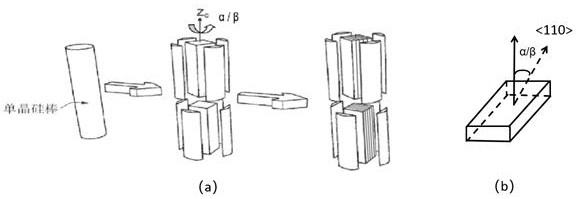
[0054] (1) Prepare a p-type single crystal silicon short round rod with a crystal orientation, a diameter of 240mm, and a length of 500mm grown by the pulling method. Connect the intersection of four ridgelines and the end face on the end face of the round rod to form a square, and place the square along the axis After rotating 45°, rotate the square by 5°. Cut along the four sides of the rotated square to obtain a 170mm*170mm*500mm single crystal square rod, cut the single crystal square rod longitudinally to obtain a 170mm*500mm*10mm long plate, and clean the long plate to obtain a single crystal silicon seed crystal long plate.

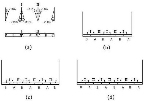
[0055] (2) Spray silicon nitride release agent on the inner surface of the crucible for ingot casting (inner bottom 1050mm*1050mm, square); remove the 10-15mm ingot remaining on the side wall of the crucible with 12 single crystal seed crystal long plates outside the safety clearance, follow the figure 1 (c) shows that the inner bottom of the cru...

Embodiment 2

[0058] (1) Prepare an n-type single crystal silicon short round rod with a crystal orientation, a diameter of 270mm, and a length of 1330mm grown by the pulling method. Connect the intersections of four ridgelines and the end face on the end face of the round rod to form a square, and place the square along the axis After rotating 45°, rotate the square by 5°. Cut along the four sides of the rotated square to obtain a 190mm*190mm*1330mm single crystal square rod, and longitudinally cut the single crystal square rod to obtain a 190mm*1330mm*15mm long plate. After cleaning the long plate, a single crystal silicon seed crystal long plate is obtained, which is marked as seed crystal A.

[0059] (2) Prepare n-type single crystal silicon short round rods with crystal direction, diameter 270mm, and length 1330mm grown by pulling method, connect four ridgelines on the end face of the round rod and the intersection points of the end face to form a square, and place the square along t...

Embodiment 3

[0063] (1) Prepare an n-type single crystal silicon short round rod with a crystal orientation, a diameter of 285mm, and a length of 1200mm grown by the pulling method. Connect the intersection of four ridgelines and the end face on the end face of the round rod to form a square, and place the square along the axis After rotating by 45°, rotate the square by 15°. Cut along the four sides of the rotated square to obtain a 200mm*200mm*1200mm single crystal square rod, and longitudinally cut the single crystal square rod to obtain a 200mm*1200mm*20mm long plate. After cleaning the long plate, a single crystal silicon seed crystal long plate is obtained.

[0064] (2) Spray silicon nitride release agent on the inner surface of the ingot crucible (inner bottom 1230mm*1230mm, square). Remove the 10-15mm ingot safety gap left between the 6 single crystal seed crystal long plates and the side wall of the crucible, according to figure 1 (b) shows that the inner bottom of the crucible...


PUM

PropertyMeasurementUnit
widthaaaaaaaaaa

Abstract

The invention provides a laying method for casting monocrystalline silicon seed crystals. The <110> crystal orientation of adjacent silicon seed crystals points to or is far away from splicing seams obliquely upwards at a smaller acute angle, and the two types of splicing seams are regularly distributed at intervals. <110> crystal orientation obliquely upward pointing splicing seams of the siliconseed crystals on the two sides can significantly inhibit generation and expansion of dislocation in the crystal growth process, and the overall crystal quality of the silicon ingot is improved. The invention also provides a crystalline silicon ingot prepared by using the laying method of the monocrystalline silicon seed crystal and a cutting and squaring method of the crystalline silicon ingot, which can be used for removing the dislocation generated by a seed crystal splicing seam, improving the proportion of a slicing part of the silicon ingot, reducing the cost of a silicon wafer and facilitating the preparation of a large-size silicon wafer. The problem of rapid dislocation propagation at the seed crystal splicing seam during production of monocrystalline silicon by a casting method is solved, and the prepared crystalline silicon solar cell is high in efficiency, centralized in distribution and consistent in appearance color, and has a remarkable market application value.

Description

technical field [0001] The invention belongs to the technical field of crystalline silicon growth, and in particular relates to a method for laying cast monocrystalline silicon seed crystals, a crystalline silicon ingot and a method for cutting and square-cutting the crystalline silicon ingot. Background technique [0002] In the solar photovoltaic industry, crystalline silicon is the most widely used solar cell material. According to the different crystal structures of crystalline materials, crystalline silicon can be divided into two types: monocrystalline silicon and polycrystalline silicon. It is generally believed that the monocrystalline silicon prepared by the Czochralski method has good structural integrity and high photoelectric conversion efficiency, but the preparation cost is high; the polycrystalline silicon prepared by the casting method is low in cost, but has many crystal structure defects and low photoelectric conversion efficiency. In recent years, the gro...

Claims


Application Information

Patent Timeline
Patent Type & Authority Applications(China)
IPC IPC(8): C30B11/14C30B29/06
CPCC30B11/14C30B29/06
Inventor 黎金香
Owner 黎金香
Why Eureka
Try Eureka