Self-driven integrated photochromic assembly energy-saving glass
An energy-saving glass, integrated technology, applied in the direction of photovoltaic power generation, electrical components, electrical solid devices, etc., can solve the problems of high installation cost, a lot of manpower and material resources, etc., achieve simple manufacturing process, simple preparation process, optimize energy and The effect of optical modulation management
- Summary
- Abstract
- Description
- Claims
- Application Information
AI Technical Summary
Problems solved by technology
Method used
Image
Examples
preparation example Construction
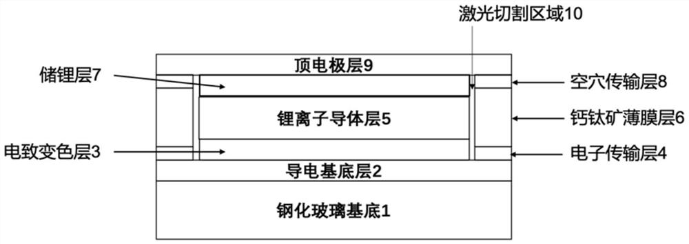
[0042] The preparation method of the self-driven integrated photochromic component energy-saving glass includes the following steps:
[0043] 1) Preparing a tin-doped indium oxide (ITO) layer or a fluorine-doped tin oxide (FTO) layer on a transparent glass substrate; the preparation may use a magnetron sputtering process.
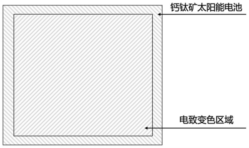
[0044] 2) Preparation of Li-doped tungsten oxide layer on ITO (Li:WO 3 ); The preparation of Li-doped tungsten oxide layer on ITO (Li:WO 3 ) can adopt magnetron sputtering or wet processing method; the tungsten oxide layer (Li:WO) doped with Li 3 ) layer is used for both perovskite solar cells and electrochromic parts; the part belonging to perovskite solar cells is used as an electron transport layer with a thickness of 10-80nm (tungsten oxide layer doped with Li (Li:WO 3 ) can be tin oxide (SnO 2 ) layer or titanium oxide layer (TiO 2 ) instead); the electrochromic layer 3 belonging to the electrochromic part has a thickness of 10-300 nm. The pattern...
Embodiment 1
[0051] The method for preparing energy-saving glass for self-driven integrated photochromic components according to the embodiment of the present invention includes the following steps:
[0052] 1) A layer of ITO film is deposited on the ultra-thin glass sheet (tempered glass substrate 1) by magnetron sputtering process, the film thickness is 180nm, and the overall size is 10cm×10cm.
[0053] 2) Magnetron sputtering is used to deposit lithium-doped tungsten oxide on the ITO, and a stainless steel mask is used to control the thickness of the electrochromic layer 3 to 100nm; similarly, the thickness of the electron transport layer 4 in the solar cell area is controlled 30nm.
[0054] 3) Formamidine lead iodide perovskite film layer 6 (Cs 0.05 FA 0.95 PB 3 ), combined with the high-speed airflow method for crystallization, the thickness is about 350nm.
[0055] 4) Deposit LiPON with a thickness of 200nm in the electrochromic region using a stainless steel mask using a magnetr...
Embodiment 2
[0063] Similar to Example 1, the difference lies in Step 2, Step 4-6:
[0064] 1) A layer of ITO film is deposited on the ultra-thin glass sheet (tempered glass substrate 1) by magnetron sputtering process, the film thickness is 180nm, and the overall size is 10cm×10cm.
[0065] 2) Magnetron sputtering is used to deposit lithium-doped tungsten oxide on the ITO, and a stainless steel mask is used to control the thickness of the electrochromic layer 3 to 100nm; similarly, an inkjet printing process is used to deposit the tin oxide electron transport layer 4 The thickness is 30nm.
[0066] 3) Formamidine lead iodide perovskite film layer 6 (Cs 0.05 FA 0.95 PB 3 ), combined with the high-speed airflow method for crystallization, the thickness is about 350nm.
[0067] 4) Deposit LiPON with a thickness of 300nm in the electrochromic region using a stainless steel mask using a magnetron sputtering process.
[0068] 5) Deposit nickel oxide with a thickness of 130 nm in the electr...
PUM
| Property | Measurement | Unit |
|---|---|---|
| thickness | aaaaa | aaaaa |
| thickness | aaaaa | aaaaa |
| thickness | aaaaa | aaaaa |
Abstract
Description
Claims
Application Information


