
Scaln/gan high electron mobility transistor and method of making same

A high electron mobility, transistor technology, applied in semiconductor/solid-state device manufacturing, circuits, electrical components, etc., can solve problems such as limiting the operating frequency of HEMT devices, deteriorating reliability, affecting device current and power output characteristics, and achieving improvement Device current and power output characteristics, improving device current and power characteristics, and eliminating the effect of the reverse piezoelectric effect

Active Publication Date: 2022-03-04
XIDIAN UNIV
View PDF5 Cites 0 Cited by
  • Summary
  • Abstract
  • Description
  • Claims
  • Application Information

AI Technical Summary

Problems solved by technology

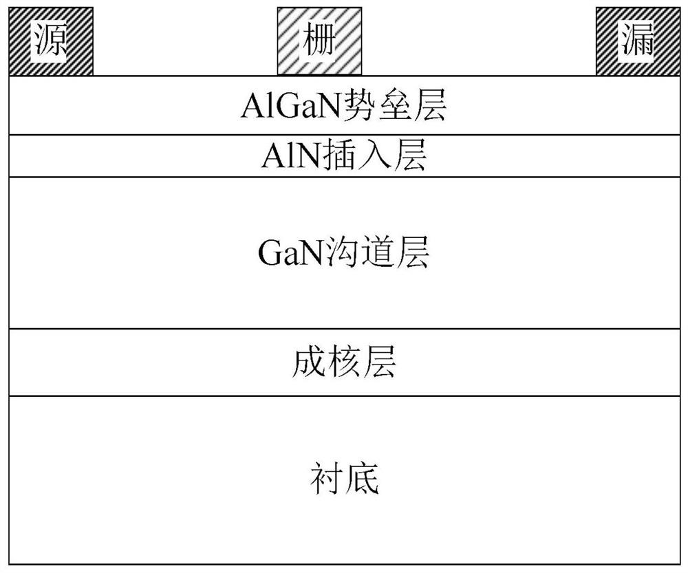
[0004] One is that in the process of heteroepitaxial GaN materials, high-density dislocation defects are inevitably generated, which will form leakage channels when the device works at high voltage for a long time, reducing the breakdown voltage of the device and deteriorating reliability;
[0005] The second is that there is a large lattice mismatch and tensile strain in the AlGaN barrier layer and the GaN channel layer. When the device works at high voltage, an inverse piezoelectric effect occurs in the AlGaN barrier layer, forming lattice defects and reducing device reliability;
[0006] The third is that the two-dimensional electron gas concentration generated by the polarization effect at the AlGaN / GaN heterojunction interface is not high enough, which limits its application in the field of high-frequency and high-power devices;
[0007]Fourth, if the AlGaN barrier layer is not protected, surface states will be generated on the surface of the barrier layer, which will reduce the concentration of two-dimensional electron gas and affect the current and power output characteristics of the device
[0008] Fifth, the thick AlGaN barrier layer needs to increase the gate length to effectively control the channel two-dimensional electron gas, which limits the improvement of the operating frequency of HEMT devices
[0009] Sixth, the source-drain electrodes are made directly on the surface of the AlGaN barrier layer. The ohmic contact resistance of the source-drain region is very high, which affects the current and power output characteristics of the device.

Method used


Image

  • Scaln/gan high electron mobility transistor and method of making same
  • Scaln/gan high electron mobility transistor and method of making same
  • Scaln/gan high electron mobility transistor and method of making same

Examples


Embodiment 1

[0054] Embodiment one, the production adopts In 0.14 Al 0.86 N cap layer, Sc 0.15 Al 0.85 Sapphire-based ScAlN / GaN high electron mobility transistor with N barrier layer.

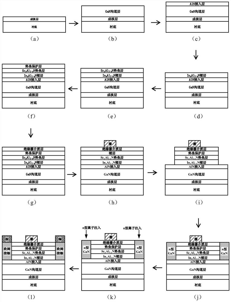
[0055] Step 1, epitaxial AlN nucleation layer, such as image 3 (a).

[0056] A metal-organic chemical vapor deposition technique was used to epitaxially form an AlN nucleation layer with a thickness of 100 nm on a sapphire substrate.

[0057] The process conditions used for the epitaxial AlN nucleation layer are: temperature 1200° C., pressure 40 Torr, ammonia gas flow rate 2000 sccm, aluminum source flow rate 20 sccm, and hydrogen gas flow rate 3000 sccm.

[0058] Step 2, depositing a GaN channel layer, such as image 3 (b).

[0059] A GaN channel layer with a thickness of 3000 nm was deposited on the AlN nucleation layer using metal organic chemical vapor deposition technique.

[0060] The process conditions for depositing the GaN channel layer are as follows: temperature is 1080°C, pressure is 4...

Embodiment 2

[0086] Embodiment two, the production adopts In 0.2 Al 0.8 N cap layer, Sc 0.2 Al 0.8 Silicon-based ScAlN / GaN high electron mobility transistor with N barrier layer.

[0087] Step 1, epitaxial AlN and AlGaN and AlGaN / GaN superlattice composite nucleation layer using metal-organic chemical vapor deposition technology, such as image 3 (a).

[0088] (1a) under the process conditions that the temperature is 1100°C, the pressure is 40 Torr, the flow rate of ammonia gas is 2000 sccm, the flow rate of aluminum source is 20 sccm, and the flow rate of hydrogen gas is 3000 sccm, an AlN nucleation layer with a thickness of 60 nm is epitaxially formed on the silicon substrate;

[0089](1b) The temperature is 1100°C, the pressure is 40 Torr, the ammonia gas flow rate is 2000 sccm, the aluminum source flow rate is 20 sccm, the gallium source flow rate is 120 sccm, and the hydrogen gas flow rate is 3000 sccm, and the deposition thickness on the AlN nucleation layer is 80nm AlGaN nuclea...

Embodiment 3

[0112] Embodiment three, the production adopts In 0.17 al 0.83 N cap layer, Sc 0.18 al 0.82 Silicon carbide-based ScAlN / GaN high electron mobility transistor with N barrier layer.

[0113] Step A, epitaxial AlN nucleation layer, such as image 3 (a).

[0114] Using metal-organic chemical vapor deposition technology, set the temperature at 1150°C, pressure at 40Torr, flow rate of ammonia gas at 2000sccm, flow rate of aluminum source at 30sccm, flow rate of hydrogen gas at 3000sccm, and deposit a thickness of 120nm on the silicon carbide substrate high temperature AlN nucleation layer.

[0115] Step B, deposit GaN channel layer, such as image 3 (b).

[0116] Using metal-organic chemical vapor deposition technology, under the process conditions of temperature 1150°C, pressure 40Torr, ammonia gas flow rate 2000 sccm, gallium source flow rate 100 sccm, hydrogen gas flow rate 3000 sccm, the thickness of the AlN nucleation layer is deposited as follows: 1500nm GaN channel la...


PUM

PropertyMeasurementUnit
thicknessaaaaaaaaaa
thicknessaaaaaaaaaa
thicknessaaaaaaaaaa

Abstract

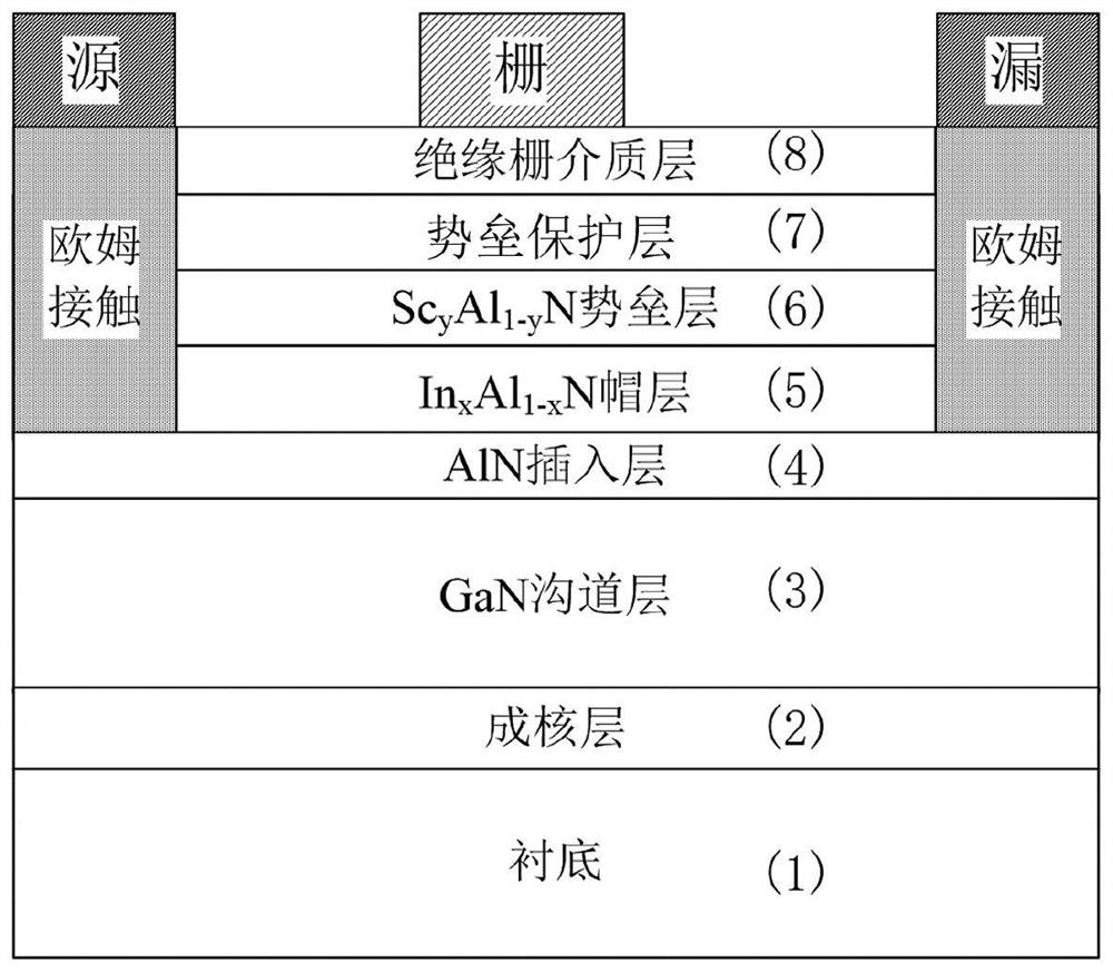
The invention relates to a ScAlN / GaN high electron mobility transistor and a manufacturing method thereof, and mainly solves the problems of current leakage at the homogeneous epitaxial interface and low operating frequency of existing nitride microwave power devices. It includes a substrate, a nucleation layer, a GaN channel layer, an AlN insertion layer and a ScAlN barrier layer from bottom to top, and an InAlN cap layer is arranged between the insertion layer and the barrier layer; The barrier protection layer and the insulating gate dielectric layer are provided with ohmic contact regions for making source and drain electrodes on both sides of the InAlN cap layer to the insulating gate dielectric layer. The nucleation layer, GaN channel layer, AlN insertion layer and InAlN cap layer in this structure are grown by MOCVD; ScAlN barrier layer and barrier protection layer are grown by MBE. The invention has no parasitic leakage at the homogeneous epitaxial interface, high operating frequency of the device, high output current density and simple manufacturing process, and can be used for high-frequency microwave power amplifiers and microwave millimeter-wave integrated circuits.

Description

technical field [0001] The invention belongs to the technical field of semiconductor devices, and in particular relates to a high electron mobility transistor, which can be used for making microwave power amplifiers and microwave millimeter wave monolithic integrated circuits. Background technique [0002] GaN heterojunction materials have excellent properties such as wide bandgap, high critical breakdown field strength, high electron saturation drift velocity, and two-dimensional electron gas with high electron mobility characteristics produced by strong spontaneous and piezoelectric polarization effects. The properties of materials have been extensively studied, and they have unique advantages in the application of high-frequency, high-power, and high-efficiency solid-state microwave power devices. Since the first GaN high electron mobility transistor (HEMT) prototype device was successfully prepared in 1993, relevant researchers at home and abroad have conducted extensive...

Claims


Application Information

Patent Timeline
Patent Type & Authority Patents(China)
IPC IPC(8): H01L29/06H01L29/20H01L29/778H01L21/336
CPCH01L29/0611H01L29/2003H01L29/778H01L29/66462
Inventor 薛军帅刘芳张进成郝跃李蓝星孙志鹏张赫朋杨雪妍姚佳佳
Owner XIDIAN UNIV
Learn More