
Method for preparing optical waveguide micro-lens array and detecting optical performance

A micro-lens array, optical performance technology, applied in the testing of optical performance, optical instrument testing, optics, etc., can solve the problems of increasing the difficulty of the crystal cone processing, the improvement of optical crosstalk without in-depth analysis, etc., to achieve a short cycle and ensure uniformity. , the effect of accurate detection

Active Publication Date: 2021-04-02
XI AN JIAOTONG UNIV
View PDF11 Cites 0 Cited by
  • Summary
  • Abstract
  • Description
  • Claims
  • Application Information

AI Technical Summary

Problems solved by technology

Some people have prepared crystal cone structures in different material combinations, but this combined structure increases the processing difficulty of crystal cones; some people have prepared integrated polymer cones in curved compound eyes by using air pressure assisted technology and soft lithography technology. structure, which realized the preparation of artificial compound eyes with microlenses, polymer cones and waveguides aligned. This integrated structure also avoided the coupling error caused by the combined structure, but they only focused on the effect of process parameters on the length of the polymer cone. Insufficient research on the effect of polymer cones on the optical performance of bionic compound eyes, and no in-depth analysis on the improvement of optical crosstalk

Method used


Image

  • Method for preparing optical waveguide micro-lens array and detecting optical performance
  • Method for preparing optical waveguide micro-lens array and detecting optical performance
  • Method for preparing optical waveguide micro-lens array and detecting optical performance

Examples


Embodiment Construction

[0031] The present invention will be described in detail below in conjunction with the accompanying drawings and embodiments.

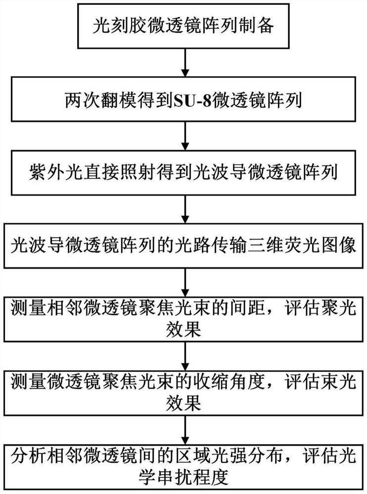
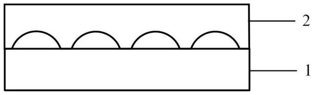
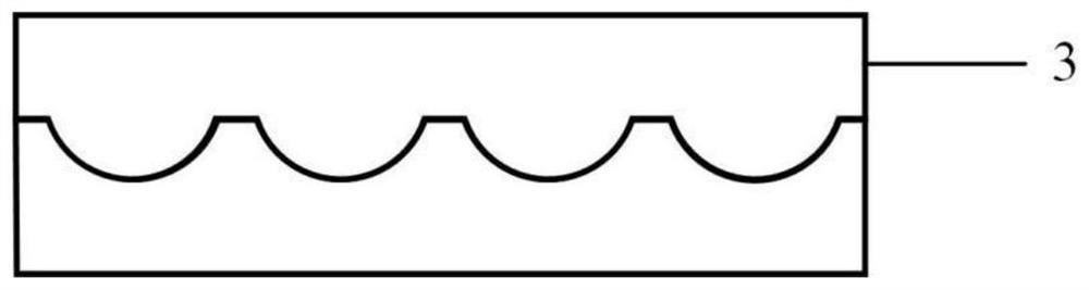
[0032] refer to figure 1 , a method for preparing an optical waveguide microlens array and detecting optical properties, comprising the following steps:

[0033] Step 1, prepare a photoresist microlens array on the glass substrate 1: wash the glass substrate with acetone, absolute ethanol, and deionized water for 10 minutes, and place the cleaned glass substrate 1 on a hot plate at 120°C Heating for 20 minutes; spin coating photoresist on the glass substrate 1, the photoresist is AZ4620, the spin coating parameters are 10s at a low speed of 500r / min, and 40s at a high speed of 3000r / min, to obtain a photoresist with a film thickness of about 10μm Adhesive film, after exposure under the photolithography machine, develop to obtain a columnar array, the exposure parameters are: the exposure power density is 10mW / cm 2 , the exposure time is 15s, and the...


PUM

PropertyMeasurementUnit
diameteraaaaaaaaaa
heightaaaaaaaaaa
wavelengthaaaaaaaaaa

Abstract

The invention relates to a method for preparing an optical waveguide micro-lens array and detecting optical performance, the method comprises the following steps: preparing a photoresist micro-lens array, mixing polydimethylsiloxane and a curing agent, pouring the mixed polydimethylsiloxane and curing agent into the photoresist micro-lens array, and curing and stripping to obtain a concave lens array reverse mold; covering the surface of a heated SU-8 with the concave lens array reverse mold, quickly imprinting, cooling and stripping to obtain an SU-8 micro-lens array; directly irradiating theSU-8 micro-lens array by using ultraviolet light to prepare an optical waveguide micro-lens array; then, in a fluorescence observation state, selecting a fluorescent dye in a laser confocal microscope, setting a scanning depth and a scanning step length to obtain a light path transmission three-dimensional fluorescence image of the optical waveguide micro-lens array, and judging whether an optical waveguide structure is induced in the SU-8 micro-lens array or not by analyzing the distribution area of focusing light spots; and finaly, performing the evaluation of optical performance of the optical waveguide micro-lens array. According to the invention, the preparation of the optical waveguide micro-lens array is realized, and the optical performance of the optical waveguide micro-lens array is detected and evaluated.

Description

technical field [0001] The invention relates to the technical field of micro-nano manufacturing, in particular to a method for preparing an optical waveguide micro-lens array and detecting optical properties. Background technique [0002] In order to realize the transmission and change of optical information, the micro-optical imaging system was born. With the development of optical information processing and optical computing technology, the micro-optical imaging system is developing in the direction of simplicity, miniaturization, and compactness. A wide field of view ( FOV), high resolution, and high motion sensitivity. Microlens arrays have the advantages of light weight, small size, compact structure, and excellent optical performance. They are used in other micro-optical imaging systems such as fiber coupling, light intensity modulation, solar cells, artificial compound eyes, and biological observation. The included angle is smaller than the overall field of view, and...

Claims


Application Information

Patent Timeline
Patent Type & Authority Applications(China)
IPC IPC(8): G02B3/00G02B21/00G01M11/02
CPCG02B3/0012G02B3/0031G01M11/0285G01M11/02G02B21/0076G02B21/0036
Inventor 王文君杨雯梅雪松崔健磊刘斌凡正杰段文强
Owner XI AN JIAOTONG UNIV
Features
  • Generate Ideas
  • Intellectual Property
  • Life Sciences
  • Materials
  • Tech Scout
  • Unparalleled Data Quality
  • Higher Quality Content
  • 60% Fewer Hallucinations
Learn More