
Method for preparing high-purity silicon by recovering silicon wafer cutting waste

A technology for silicon wafer cutting and waste recycling, applied in chemical instruments and methods, silicon compounds, waste treatment, etc., can solve the problems of low impurity removal rate and serious secondary oxidation, so as to overcome secondary oxidation, improve recovery rate, The effect of reducing energy consumption in production

Active Publication Date: 2021-06-25
KUNMING UNIV OF SCI & TECH
View PDF8 Cites 4 Cited by
  • Summary
  • Abstract
  • Description
  • Claims
  • Application Information

AI Technical Summary

Problems solved by technology

[0004] The invention aims at the problems of secondary pollution in the pretreatment process of the existing silicon wafer cutting waste recycling process, low impurity removal rate in smelting and purification, serious secondary oxidation, and segmentation of smelting and refining, and provides a silicon wafer cutting waste recycling process. The method for preparing high-purity silicon, the invention uses the silicon wafer cutting waste generated during the diamond wire cutting process of solar cell silicon wafers as raw materials, first obtains low-impurity and low-oxidation raw materials through pretreatment, and then uses vacuum remelting and vacuum refining, The vacuum ingot casting process realizes the removal of impurities in the silicon melt and prepares 6N grade silicon

Method used


Image

  • Method for preparing high-purity silicon by recovering silicon wafer cutting waste
  • Method for preparing high-purity silicon by recovering silicon wafer cutting waste

Examples


Embodiment 1

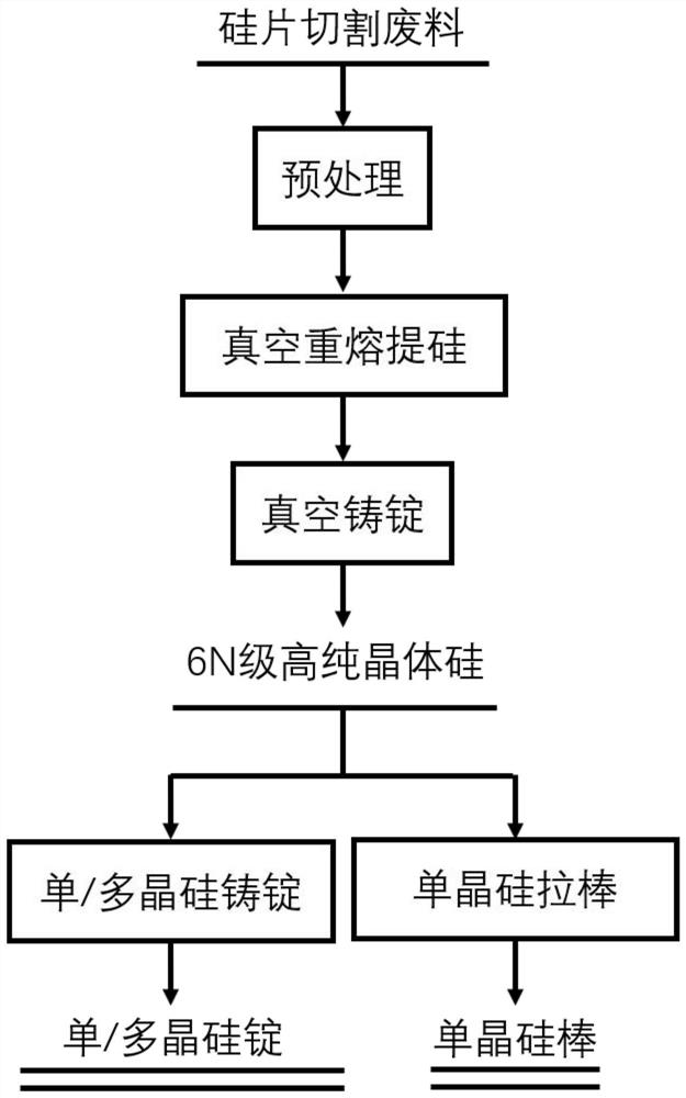
[0030] Example 1: A method of preparing high purity silicon in a wafer cutting waste (see figure 1 ),Specific steps are as follows:

[0031] (1) Put the fresh silicon sliced ​​waste slurry of a single crystal silicon slice enterprise in Yunnan, a vacuum dry dehydration to constant weight to obtain a silicon cutting waste, wherein the vacuum drying temperature is 60-80 ° C, and the vacuum pressure of vacuum drying is not higher than the vacuum drying temperature. -0.6bar, the impurity content in silicon cutting waste is Al 53 ppmw, Fe 300 ppmw, Ni 51PPMW, Ti 80.5 ppmw, Ca 50 ppmw, mg15ppmw, b 5.4 ppmw, p 10 ppmw, total impurity content of 564.9 ppmw;

[0032] (2) Transfer the wafer cutting waste to the graphite crucible and compact, put the graphite 坩 坩 感 感 感 感 感 加 定 定 定 定 定 定 处理 定 定 定 定 处理 处理 定 定 定 定 放 放After the furnace is lower than 50Pa, the heating is turned on, and the temperature rise time is about 0.5 h, so that the wafer cuts the waste, heat-insulation refining under vacuu...

Embodiment 2

[0035] Example 2: Method for preparing high purity silicon by silicon cutting waste recovery (see figure 1 ),Specific steps are as follows:

[0036] (1) After the wafer cutting, settling, pressure filtering, and flame retardant liquid, the silicon plate cutting waste slurry is directly separated, wherein the wet treatment process is vacuum. The two glyphs were acidic under conditions, of which one acidic leach was 2 m HCl + 2.5 M HF mixed acid, the leaching temperature was 60 ° C, the leaching time was 3 h, and the solid-liquid separation was performed after the leaching, and then the segment leaching was carried out. 4M HCl, the leaching temperature is 60 ° C, the leaching time is 3 h, and the second-stage leaching is faster under vacuum conditions, dehydrated and dried. After two segments, the average content of the aburmented wafer cutting waste after the two sections is Al 61.5 ppmw, Fe 38.5PPMW, Ni 46.5 ppmw, Ti 4.8ppmw, Ca 18ppmw, Mg5PPMW, B 5PPMW, P10 PPMW, total impurity c...

Embodiment 3

[0040] Example 3: Method for preparing high purity silicon by wafer cutting waste (see figure 1 ),Specific steps are as follows:

[0041] (1) Cut the silicon wafer of a single crystal silicon slice enterprise in Yunnan to dehydrate to constant weight, wherein the vacuum drying temperature is 60-80 ° C, and the vacuum pressure of vacuum drying is not higher than -0.6 bar, wafer cutting waste. The impurity content is AL53PPMW, Fe 300 ppmw, Ni 51PPMW, Ti 80.5 ppmw Ca 50 ppmw mg 15 ppmw, b 5.4 ppmw, p10 ppmw, total impurity content of 564.9 ppmw;

[0042] (2) Transfer the wafer cutting waste to the graphite crucible and compact, put the graphite 坩 坩 感 感 感 感 感 加 定 定 定 定 定 定 处理 定 定 定 定 处理 处理 定 定 定 定 放 放After the furnace is below 50Pa, the heating is turned on, and the temperature rise is about 0.5 h to cut the wafer cutting waste, and the refined refining is insulated under vacuum, temperature 1550-1600 ° C. After the insulation, the furnace is cooled.

[0043] (3) Cut the silicon ingot...


PUM

PropertyMeasurementUnit
particle sizeaaaaaaaaaa

Abstract

The invention relates to a method for preparing high-purity silicon by recovering silicon wafer cutting waste, and belongs to the technical field of high-value recycling of silicon resources. Based on the characteristics of high content of high-purity silicon in the silicon wafer cutting waste, surface oxidation and metal impurity enrichment surface, the invention provides a method for directly preparing high-purity silicon from the silicon wafer cutting waste by vacuum smelting refining and vacuum directional ingot casting purification. Fresh silicon wafer cutting waste is used as a raw material, pretreatment is carried out under oxygen isolation or inert gas, the silicon wafer cutting waste is melted, slagged-off and refined under the vacuum condition, then vacuum directional ingot casting purification of silicon melt is carried out, and a high raw silicon product with the purity higher than 6N level is obtained. The obtained high raw silicon product with the purity higher than 6N grade can be directly or mixed for single crystal drawing and casting single / polycrystalline silicon crystal growth, and has the advantages of being simple in equipment requirement, free of additives, short in process, high in product additional value, easy to operate and suitable for large-scale industrial production.

Description

Technical field [0001] The present invention relates to a method of preparing high purity silicon by a silicon-cutting waste recovery, belonging to the technical field of silicon resource high value regeneration utilization. Background technique [0002] In photovoltaic solar cells, crystalline silicon solar cells are the most widely used photoelectric conversion material. However, in the current solar cell silicon production process, about 30-40% high-purity crystalline silicon is inevitable in the form of a silicon-cutting waste in the form of a silicon wire cutting pulp and cannot be recovered. In the existing diamond line cutting slurry, in order to reduce the solid-liquid separation operation difficulty and shorten the separation cycle, it is necessary to add a plurality of additives for flocculation and settlement treatment, and in order to avoid and prevent the water-containing wafer cutting waste after solid-liquid separation or Spike also needs further spray flame retard...

Claims


Application Information

Patent Timeline
Patent Type & Authority Applications(China)
IPC IPC(8): C01B33/037C30B11/00C30B15/00C30B29/06
CPCC01B33/037C30B11/00C30B15/00C30B29/06Y02W30/20
Inventor 马文会杨时聪魏奎先邓小聪
Owner KUNMING UNIV OF SCI & TECH
Learn More