
Nano silicon material and preparation method thereof

A technology of nano-silicon and silicon materials, applied in nanotechnology, nanotechnology, chemical instruments and methods, etc., can solve problems such as harsh process conditions, difficulty in maintaining cycle performance, and difficulty in large-scale production

Pending Publication Date: 2021-07-16
江苏载驰科技股份有限公司
View PDF2 Cites 1 Cited by
  • Summary
  • Abstract
  • Description
  • Claims
  • Application Information

AI Technical Summary

Problems solved by technology

However, the above-mentioned material synthesis methods are mainly chemical vapor deposition, laser ablation, electron beam evaporation, magnetron sputtering, and metal-assisted chemical etching. However, these preparation methods have extremely high requirements for equipment, harsh process conditions, Mainly use silane or silicon tetrachloride as silicon source, high cost and difficult to scale production
Most of the nano-materials prepared by the above method are crystalline nano-silicon, and the volume expansion has anisotropy during charge and discharge, resulting in uneven distribution of mechanical stress, which is easy to cause material cracking and crushing, and it is difficult to maintain long-term cycle performance.

Method used


Image

  • Nano silicon material and preparation method thereof
  • Nano silicon material and preparation method thereof
  • Nano silicon material and preparation method thereof

Examples


Embodiment 1

[0063] Boron-doped P-type single crystal silicon material (resistivity 0.01 Ω cm) is used as workpiece electrode and tool electrode. The workpiece electrode is a cuboid with a thickness of 20mm, and the tool electrode is a square with a cross section of 5mm*5mm, and a through hole with a diameter of 2mm in the middle The working fluid is insulating deionized water (resistivity 10 MΩ·cm).

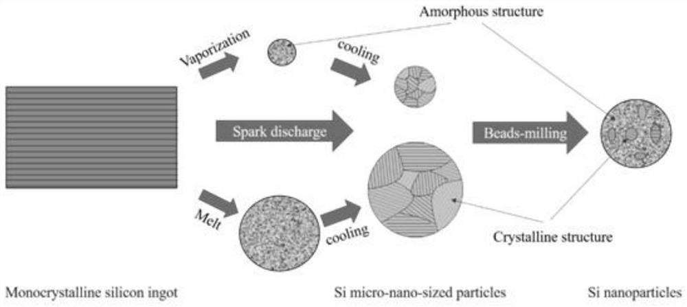
[0064] The pulse width of the discharge pulse generated by the pulse power supply is 200μs and 200ns respectively, the duty ratio is 1:4, and the rectangular pulse voltage with an open circuit voltage of 160V is applied between the workpiece electrode and the tool electrode, ionizing and breaking down the insulating working medium to form a plasma discharge Channel, the resulting high-temperature melting and gasification workpiece electrodes are condensed to obtain micron and submicron silicon materials with amorphous / nanocrystalline composite structure. After filtering with a centrifuge to ...


PUM

PropertyMeasurementUnit
Thicknessaaaaaaaaaa
Particle sizeaaaaaaaaaa

Abstract

The invention relates to a nano silicon material with an amorphous / nanocrystalline composite structure. In the application of a lithium / sodium ion battery, after lithium / sodium is embedded into a crystalline silicon material for the first time, a composite structure of an amorphous region (silicon-lithium alloy) and a crystalline region (not embedded with lithium) is formed, and volume expansion and structural change are generated; after lithium / sodium removal, volume shrinkage causes structure collapse, i.e., silicon particle fracture and pulverization. In order to provide enough lithium / sodium embedding space in advance and inhibit the volume change of lithium / sodium embedding / removal for the first time, the invention provides an amorphous / nanocrystalline composite structure and a controllable preparation method thereof, i.e., a nano silicon material with the amorphous / nanocrystalline composite structure is prepared by adopting a spark discharge and high-energy ball milling combined process, the amorphous region surrounds the nanocrystalline, the crystal face orientation of the nanocrystalline is randomly distributed, the proportion range of the amorphous region is controllable, and the amorphous region belongs to an isotropic material. In the application of lithium and sodium ion batteries, the structure can effectively relieve the problems of material fracture and pulverization caused by silicon material expansion / shrinkage due to embedding / removal of lithium / sodium, so that the cycle performance of the silicon negative electrode is improved.

Description

technical field [0001] The invention relates to a nano-silicon material with an amorphous / nano-crystalline composite structure, and belongs to the technical field of negative electrode materials for lithium batteries. Background technique [0002] In recent years, with the rapid development of new energy pure electric vehicles, plug-in hybrid electric vehicles and electric tools, higher requirements have been placed on the energy density, safety and cycle stability of lithium-ion batteries. Graphite is used as a commercial anode material for lithium-ion batteries (theoretical specific capacity is 372 mAh g -1 ), has been unable to meet the market demand for large batteries with high energy density. Silicon-based anode materials have a high theoretical specific capacity of 4200 mAh g -1 , lower charge and discharge platform (close to the potential platform of graphite), green environmental protection and high safety, etc., is considered to be the most lithium-ion battery ...

Claims


Application Information

Patent Timeline
IPC IPC(8): H01M4/36H01M4/38H01M10/0525C01B33/02C01B33/021B82Y30/00B82Y40/00
CPCH01M4/364H01M4/386H01M10/0525C01B33/02C01B33/021B82Y30/00B82Y40/00Y02E60/10
Inventor 赵明才张娟汪炜
Owner 江苏载驰科技股份有限公司
Learn More