Electron transport material ink for ink-jet printing, and preparation method and application thereof

An electronic transmission material and inkjet printing technology, applied in applications, inks, circuits, etc., can solve problems such as uneven film thickness, achieve the effects of reducing production costs, simple production process, and suppressing the formation of coffee rings

Active Publication Date: 2021-08-10
NANJING UNIV OF POSTS & TELECOMM
View PDF3 Cites 2 Cited by
  • Summary
  • Abstract
  • Description
  • Claims
  • Application Information

AI Technical Summary

Problems solved by technology

[0004] Due to the problem of mutual solubility between layers during film preparation and the non-uniform film thickness caused by the coffee ring phenomenon when preparing multilayer OLEDs by solution method, the performance index of OLED devices prepared by solution method is still lower than that of traditional vacuum evaporation devices. large gap

Method used


Image

  • Electron transport material ink for ink-jet printing, and preparation method and application thereof
  • Electron transport material ink for ink-jet printing, and preparation method and application thereof
  • Electron transport material ink for ink-jet printing, and preparation method and application thereof

Examples


Embodiment 1

[0040] Hole transport layer solution preparation: the hole transport polymer polyvinylcarbazole (PVK) was dissolved in chlorobenzene solvent, the solution concentration was 10mg / mL.

[0041] Preparation of the light-emitting layer solution: the hole transport material 4,4,4,-tris(carbazol-9-yl)triphenylamine (TCTA), the electron transport material 2,6-bis((9H-carbazol-9-yl )-3,1-phenylene)pyridine (26DCzPPy) and the green phosphorescent dye tris(2-phenylpyridine)iridium(III)(Ir(ppy) 3 ) according to being dissolved in the chlorobenzene solvent in the mass ratio of 9:9:2, solution concentration 20mg / mL.

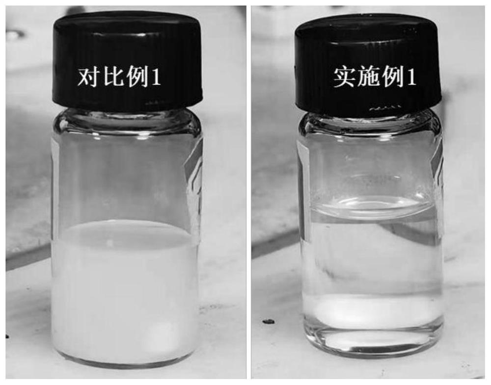
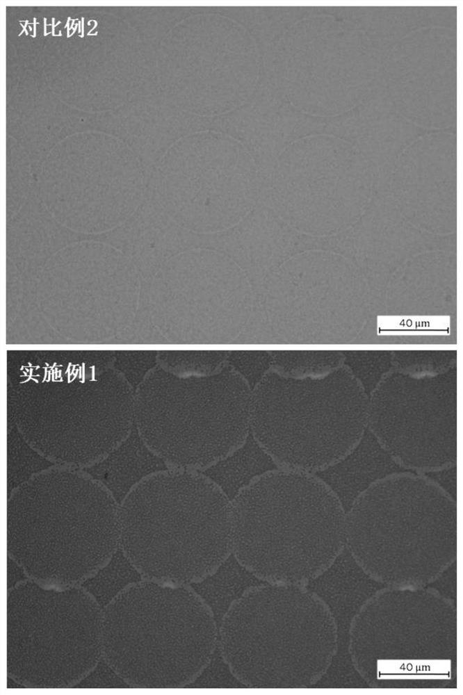
[0042] Electron transport material ink configuration: Dissolve 1,3,5-tris(1-phenyl-1H-benzimidazol-2-yl)benzene (TPBi) in isopropanol:methanol mixed solution, solution ratio 50%:50 % (volume ratio), concentration 4mg / mL.

[0043] Preparation of hole transport layer, light emitting layer and electron transport layer:

[0044] First, ultrasonically treat the ITO glass substra...

Embodiment 2

[0050] Preparation of the hole transport layer solution: Dissolve PVK in chlorobenzene solvent with a solution concentration of 10 mg / mL.

[0051] Preparation of luminescent layer solution: mix TCTA, 26DCzPPy and Ir(ppy) 3 Dissolve in chlorobenzene solvent according to the mass ratio of 9:9:2, solution concentration 20mg / mL.

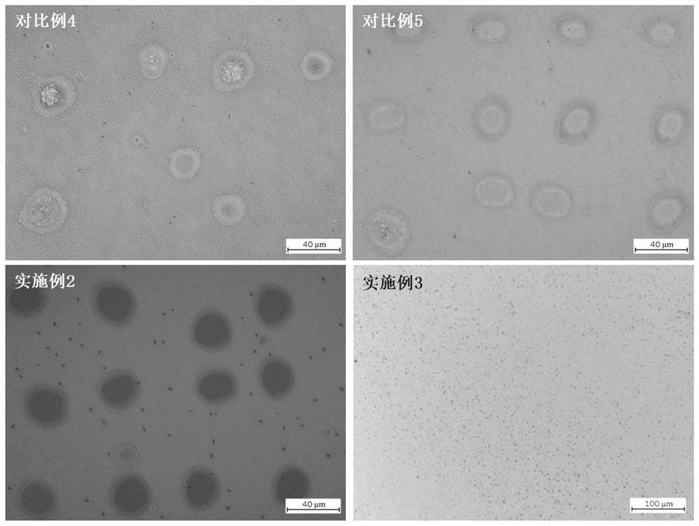
[0052] Electron transport material ink configuration: TPBi was dissolved in methanol: ethylene glycol mixed solution, solution ratio 90%: 10% (volume ratio), concentration 8mg / mL.

[0053] Preparation of hole transport layer, light emitting layer and electron transport layer:

[0054] First, ultrasonically treat the ITO glass substrate in acetone, ethanol, and deionized water for 15 minutes in sequence, blow it dry with nitrogen, and place it in an oven at 120°C for drying;

[0055] Secondly, after 15 minutes of UVO treatment, spin-coat PEDOT:PSS solution at a speed of 2500rpm, spin-coat for 1 minute, and solidify the film at 120°C for 30 minutes, with...

Embodiment 3

[0060] Preparation of the hole transport layer solution: Dissolve PVK in chlorobenzene solvent with a solution concentration of 10 mg / mL.

[0061] Preparation of luminescent layer solution: mix TCTA, 26DCzPPy and Ir(ppy) 3 Dissolve in chlorobenzene solvent according to the mass ratio of 9:9:2, solution concentration 20mg / mL.

[0062] Electronic transport material ink configuration: TPBi was dissolved in methanol: ethylene glycol: polyethylene glycol octylphenyl ether mixed solution, solution ratio 90%: 10%: 0.15% (volume ratio), concentration 8mg / mL.

[0063] Preparation of hole transport layer, light emitting layer and electron transport layer:

[0064] First, ultrasonically treat the ITO glass substrate in acetone, ethanol, and deionized water for 15 minutes in sequence, blow it dry with nitrogen, and place it in an oven at 120°C for drying;

[0065] Secondly, after 15 minutes of UVO treatment, spin-coat PEDOT:PSS solution at a speed of 2500rpm, spin-coat for 1 minute, and...


PUM

PropertyMeasurementUnit
concentrationaaaaaaaaaa
thicknessaaaaaaaaaa

Abstract

The invention discloses an electron transport material ink for ink-jet printing, and a preparation method and application thereof. The ink comprises: a solute; solvents comprising methanol and ethylene glycol; and a surfactant being polyethylene glycol octyl phenyl ether. The solute concentration of the electron transport material ink for ink-jet printing is 2-10 mg/mL, the volume ratio of methanol to ethylene glycol is (80-99): (1-20), and the volume ratio of the surfactant to the solvent is (0.1-0.15): 100. The invention provides the electron transport material ink for ink-jet printing. The problem of mutual dissolution between layers during ink-jet printing of multiple layers of films is solved by adopting an orthogonal solvent method; and the problem of poor spreadability of ink droplets on the surface of a hydrophobic light-emitting layer film is solved by adopting a strategy of adding an activator, a uniform film is obtained, and the formation of coffee rings is inhibited.

Description

technical field [0001] The invention belongs to the technical field of inkjet printing electronic transmission materials, and in particular relates to an electronic transmission material ink for inkjet printing, a preparation method and application thereof. Background technique [0002] Organic light-emitting diode (OLED) has become a new generation of display technology due to its thinness, low power consumption, high contrast ratio and high flexibility. The manufacture of traditional OLED is realized by vacuum deposition process. This technology needs to provide high-vacuum evaporation equipment and high-precision mask plate, and the material utilization rate is only 20%. It is difficult to realize low-cost, large-size OLED. Large scale preparation. [0003] Solution process, including inkjet printing, spray coating, doctor blade coating and screen printing, can significantly reduce the cost of OLED manufacturing process equipment, which has attracted widespread attention...

Claims


Application Information

Patent Timeline
Patent Type & Authority Applications(China)
IPC IPC(8): C09D11/52C09D11/36C09D11/30H01L51/00
CPCC09D11/52C09D11/36C09D11/30H10K71/135
Inventor 兰涛刘利会朴俊贤谢炬炫陈定甫陈淑芬
Owner NANJING UNIV OF POSTS & TELECOMM
Why Eureka
Try Eureka