Nitrogen polar surface gallium nitride high electron mobility transistor and manufacturing method thereof

A high electron mobility, gallium nitride technology, applied in the field of nitrogen polar surface gallium nitride high electron mobility transistors, can solve the difficulty of material nitrogen polarity control, difficult to accurately control the etching process, device reliability and reliability. Deterioration of stability and other problems, to achieve the effect of improving the output characteristics and reliability of the device, avoiding the problem of rough peeling interface, and reducing the difficulty of etching process control

Active Publication Date: 2021-08-27
XIDIAN UNIV
View PDF3 Cites 2 Cited by
  • Summary
  • Abstract
  • Description
  • Claims
  • Application Information

AI Technical Summary

Problems solved by technology

[0005]First, it is difficult to control the polarity of nitrogen during the epitaxy of gallium nitride materials on the nitrogen polar surface, and the polarity reversal is prone to occur, resulting in the appearance of gallium nitride on the gallium polar surface Material;
[0006]Secondly, the background carrier concentration of the grown nitrogen polar gallium nitride material is high, and it is easy to form a bulk leakage channel to reduce the breakdown voltage of the device, so iron doping is required Compensation of background carriers increases the difficulty of material epitaxy process control;
[0007]Third, the thermal conductivity of the substrate is low, and the heat in the active area of ​​the GaN device on the nitrogen polar surface cannot be dissipated immediately, and the heat accumulation effect leads to device reliability and stability performance deterioration, it is difficult to give full play to the advantages of the device in high-frequency and high-power applications;
[0008]Fourth, when transferring GaN devices with nitrogen polar surfaces to high thermal conductivity diamond substrates, the sacrificial layer used in traditional methods is mostly SiO2 and other materials

Method used


Image

  • Nitrogen polar surface gallium nitride high electron mobility transistor and manufacturing method thereof
  • Nitrogen polar surface gallium nitride high electron mobility transistor and manufacturing method thereof
  • Nitrogen polar surface gallium nitride high electron mobility transistor and manufacturing method thereof

Examples


Embodiment 1

[0060] Embodiment 1: Fabricate a diamond-based gallium nitride high electron mobility transistor with a SiN bonding layer and an AlGaN barrier layer.

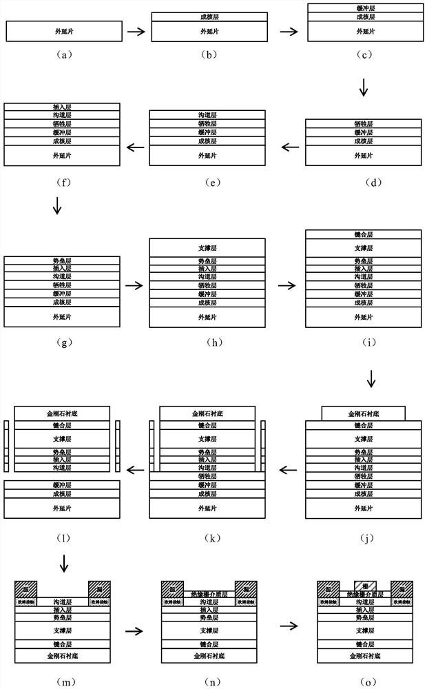
[0061] Step 1, select a sapphire epitaxial wafer as an auxiliary epitaxial substrate, such as image 3 (a).

[0062] Step 2, depositing an AlN nucleation layer, such as image 3 (b).

[0063] An AlN nucleation layer with a thickness of 140 nm was deposited on the sapphire substrate by metal organic chemical vapor deposition technique.

[0064] The process conditions for depositing the AlN nucleation layer are as follows: the temperature is 1100°C, the pressure is 40 Torr, the flow rate of ammonia gas is 2000 sccm, the flow rate of aluminum source is 20 sccm, and the flow rate of hydrogen gas is 3000 sccm.

[0065] Step 3, depositing a GaN buffer layer, such as image 3 (c).

[0066] A GaN buffer layer with a thickness of 3000 nm was deposited on the AlN nucleation layer by metal organic chemical vapor deposition technique....

Embodiment 2

[0098] Embodiment 2, manufacturing a diamond-based nitrogen polar surface gallium nitride high electron mobility transistor using a Si bonding layer and an InAlN barrier layer.

[0099] Step 1, select a silicon carbide epitaxial wafer as an auxiliary epitaxial substrate, such as image 3 (a).

[0100] Step 2, using metal organic chemical vapor deposition technique to deposit AlN nucleation layer, such as image 3 (b).

[0101] Using metal-organic chemical vapor deposition technology, under the process conditions of temperature 1200°C, pressure 40Torr, ammonia gas flow rate 2000 sccm, aluminum source flow rate 20 sccm, hydrogen gas flow rate 3000 sccm, the thickness of silicon carbide deposited on the epitaxial wafer is 100nm AlN nucleation layer.

[0102] Step 3, using metal organic chemical vapor deposition technology to deposit GaN buffer layer, such as image 3(c).

[0103] Using metal-organic chemical vapor deposition technology, under the process conditions of temper...

Embodiment 3

[0126] Embodiment 3, manufacturing a diamond-based nitrogen polar surface gallium nitride high electron mobility transistor using a SiN bonding layer and a ScAlN barrier layer.

[0127] In step A, a silicon epitaxial wafer is selected as an auxiliary epitaxial substrate, such as image 3 (a).

[0128] Step B, depositing an AlN nucleation layer, such as image 3 (b).

[0129] Using metal-organic chemical vapor deposition technology, set the temperature at 1150°C, the pressure at 40Torr, the flow rate of ammonia gas at 2000 sccm, the flow rate of aluminum source at 20 sccm, the flow rate of gallium source at 90 sccm, and the process conditions of hydrogen gas flow at 3000 sccm. Composite nucleation layer based on AlN, AlGaN, AlN / AlGaN superlattice with a product thickness of 200nm.

[0130] Step C, depositing a GaN buffer layer, such as image 3 (c).

[0131] Using metal-organic chemical vapor deposition technology, set the temperature at 1150°C, pressure at 40Torr, ammonia...


PUM

PropertyMeasurementUnit
Thicknessaaaaaaaaaa
Thicknessaaaaaaaaaa
Thicknessaaaaaaaaaa

Abstract

The invention discloses a nitrogen polar surface gallium nitride high-electron-mobility transistor and a manufacturing method thereof which mainly solve the problems that an existing nitrogen polar surface gallium nitride device is low in material epitaxial quality and can generate a heat accumulation effect and current collapse during high-voltage and high-power work. The nitrogen polar surface gallium nitride high-electron-mobility transistor comprises a diamond substrate (1), a barrier layer (4), an insertion layer (5) and a channel layer (6) from bottom to top, wherein a bonding layer (2) and a supporting layer (3) are arranged between the substrate (1) and the barrier layer (4), an insulated gate dielectric layer (7) is arranged at the upper portion of the channel layer (6), and a gate electrode is arranged on the insulated gate dielectric layer (7); ohmic contact areas are arranged at the two sides of the channel layer (6), and a source electrode and a drain electrode are arranged on the ohmic contact areas respectively. The nitrogen polar surface gallium nitride high-electron-mobility transistor is high in working frequency, the self-heating effect of a device is greatly improved, the output power working reliability of the device is improved; the manufacturing process is simple, the consistency is high, and the nitrogen polar surface gallium nitride high-electron-mobility transistor can be used for a high-frequency microwave power amplifier and a monolithic microwave millimeter wave integrated circuit.

Description

technical field [0001] The invention belongs to the technical field of semiconductor devices, in particular to a gallium nitride high electron mobility transistor on a nitrogen polar surface, which can be used for making microwave power amplifiers and monolithic microwave millimeter wave integrated circuits. Background technique [0002] The performance and reliability of microwave power amplifiers and monolithic microwave and millimeter wave integrated circuits based on gallium nitride heterojunction high electron mobility transistors have been continuously improved, and they have extremely high application value in the new generation of 5G communication base stations and electronic systems. At present, gallium nitride semiconductor devices are mainly manufactured based on gallium polar surface materials, because gallium polar surface materials are easy to achieve high-quality growth and low background carrier concentration. However, gallium nitride materials with nitrogen ...

Claims


Application Information

Patent Timeline
IPC IPC(8): H01L29/20H01L29/778H01L21/335H01L23/373
CPCH01L29/2003H01L29/778H01L29/66462H01L23/3732
Inventor 薛军帅孙志鹏吴冠霖杨雪妍李祖懋姚佳佳张进成郝跃
Owner XIDIAN UNIV
Why Eureka
Try Eureka