
Nitride high electron mobility transistor and manufacturing method thereof

A technology with high electron mobility and transistors, applied in the fields of electric solid-state devices, semiconductor/solid-state device manufacturing, circuits, etc., can solve the problem of difficult precise control of etching process, low completeness and success rate of device peeling, and rough and uneven peeling interface To achieve the effect of improving device current and power output characteristics, avoiding lattice mismatch and thermal mismatch problems, improving switching current ratio and breakdown characteristics

Active Publication Date: 2021-08-27
XIDIAN UNIV
View PDF5 Cites 0 Cited by
  • Summary
  • Abstract
  • Description
  • Claims
  • Application Information

AI Technical Summary

Problems solved by technology

[0004]First, the thermal conductivity of the substrate is low. As the size of GaN devices decreases and the power density increases, the heat accumulation effect in the active area of ​​the device increases significantly, resulting in a Performance indicators such as reliability and stability deteriorate rapidly, making it difficult to give full play to the advantages of nitride materials in high-frequency and high-power applications;
[0005] Second, there are large lattice mismatch and thermal mismatch between substrates with high thermal conductivity such as diamond and copper metals and nitride materials. It is difficult to achieve high crystalline quality for heteroepitaxially grown nitride device materials;
[0006]Third, when transferring gallium nitride devices to high thermal conductivity substrates such as diamond and copper metals, the sacrificial layer used in traditional methods is mostly SiO2 and other materials, because there is still a large lattice mismatch and thermal mismatch between the sacrificial layer and the nitride epitaxial material, the epitaxial layer on the SiO2 and other sacrificial layers Nitride materials have high-density dislocation defects, which cause the device to form a leakage channel under high-voltage long-term operation, thereby reducing the breakdown voltage of the device, and trapping electrons at the same time causes the current collapse of the device;
[0007] Fourth, the stripping process is complicated during device transfer, the etching process is difficult to control accurately, the stripping interface is rough and uneven, and the completeness and success rate of device stripping are low, resulting in Device performance degradation

Method used


Image

  • Nitride high electron mobility transistor and manufacturing method thereof
  • Nitride high electron mobility transistor and manufacturing method thereof
  • Nitride high electron mobility transistor and manufacturing method thereof

Examples


Embodiment 1

[0068] EXAMPLES First, a diamond-based nitride high electron mobility transistor using a SiN bonding layer, a GaN channel layer, and an AlGa barrier layer is produced.

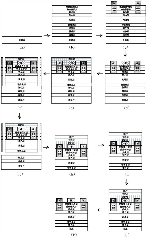
[0069] Step 1. Select sapphire epitaxial sheet as auxiliary epitaxial substrate, such as image 3 (a).

[0070] Step 2, in the sapphire epitaxial sheet, the AlN nucleation layer, GaN buffer layer, ALPN sacrificial layer, AlGan back stop layer, GaN channel layer, AlGa barrier layer, GaN barrier protective layer and Al 2 O 3 Insulated gate dielectric layer, such as image 3 (b).

[0071] 2. 1) A hydraulic layer using metal organic chemical gas phase deposition techniques on the sapphire epitaxial film, the process conditions used by the Aln nucleation layer, the process conditions employed by the Aln nucleation layer: the temperature is 1100 ° C, the pressure is 40 torr, the ammonia gas flow is 2000sccm, aluminum source of 20 sccm, hydrogen flow rate of 3000 sccm;

[0072] 2.2) A GaN buffer layer having a thickness of...

Embodiment 2

[0100] Embodiment 2, a metal copper-based nitride high electron mobility transistor using a Ti / Au bonding layer, an INGAN channel layer, and an INALN barrier layer.

[0101] Step 1, use silicon carbide epitaxial sheet, as an auxiliary epitaxial substrate, such as image 3 (a).

[0102] Step 2, in the silicon carbide epitaxial sheet, the AlN nucleation layer, GaN buffer layer, AlPn sacrificial layer, AlGan back stop layer, INGAN channel layer, INALN barrier layer, AlN barrier protective layer and HFO 2 Insulated gate dielectric layer, such as image 3 (b).

[0103] 2A) Use metal organic chemical gas phase deposition techniques, at a temperature of 1200 ° C, the pressure is 40 torr, the ammonia gas flow is 2000 sccm, the aluminum source is 20sccm, and the hydrogen flow is 3000 SCCM, the hydrogen carbide is deposited on silicon carbide. ALN-based nuclear layer having a thickness of 140 nm;

[0104] 2b) Use metal organic chemical vapor deposition techniques, at a temperature of 1200 °...

Embodiment 3

[0126] Embodiment 3 produced using Si bonding layer, a diamond-based nitride high electron mobility transistor InN ScAlN channel layer and barrier layer.

[0127] Step A, the choice of epitaxial wafers, the epitaxial substrate as an auxiliary, such as image 3 (a).

[0128] Procedure B, are sequentially grown on the silicon wafer bottom-AlN, AlGaN, AlN / AlGaN superlattice composite nucleation layer, GaN buffer layer, AlPN sacrificial layer, AlGaN barrier backing layer, GaN channel layer, ScAlN barrier layer, AlN layer and the protective barrier Al 2 O 3 Insulated gate dielectric layer, such as image 3 (b).

[0129] B1) using a metal organic chemical vapor deposition technique, a temperature of 1150 ℃, a pressure of 40 Torr, flow rate of 2000 sccm of ammonia, aluminum source flow rate of 20 sccm, 90 sccm flow rate of the gallium source, the hydrogen gas flow rate of 3000sccm process conditions, epitaxial silicon deposited in a thickness on sheet based on AlN, AlGaN, AlN / AlGaN sup...


PUM

PropertyMeasurementUnit
thicknessaaaaaaaaaa
thicknessaaaaaaaaaa
thicknessaaaaaaaaaa

Abstract

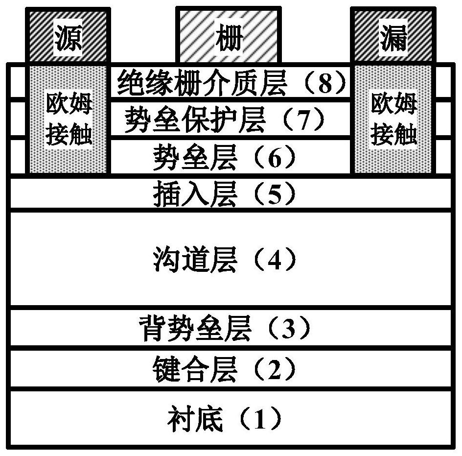
The invention discloses a nitride high-electron-mobility transistor and a manufacturing method thereof, and mainly solves the problems of heat accumulation effect and heat dissipation when an existing nitride electronic device works at high voltage and high power. The transistor comprises a high-thermal-conductivity substrate (1), a channel layer (4), an insertion layer (5) and a barrier layer (6) from bottom to top, a bonding layer (2) and a back barrier layer (3) are arranged between the substrate (1) and the channel layer (4), a barrier protection layer (7) and an insulated gate dielectric layer (8) are sequentially arranged on the upper portion of the barrier layer (6), and a gate electrode is arranged on the insulated gate dielectric layer (8); and ohmic contact areas are arranged from the insertion layer (5) to the two sides of the insulated gate dielectric layer (8), and a source electrode and a drain electrode are arranged on the ohmic contact areas respectively. The transistor is high in output power, the self-heating effect of the device is greatly improved, the heat dissipation capability and the working reliability of the device are improved, the manufacturing process is simple, the consistency is high, and the device can be used for a high-frequency microwave power amplifier and a microwave millimeter wave integrated circuit.

Description

Technical field [0001] The invention belongs to the technical field of semiconductor device, and more particularly to a nitride high electron mobility transistor, which can be used to make high frequency microwave power amplifiers and microwave millimeter wave single-chip integrated circuits. Background technique [0002] The gallium nitride semiconductor material has a large bandwidth, high high-performance, electronic saturation drift speed, microwave power devices and single-chip microwave integrated circuits based on the heterojunction of the gallium nitride heterogenesis. Increasingly improved, a high application value in the new generation of 5G communications and national defense weapons and equipment, which has attracted extensive attention from international research institutions. With the improvement and improvement of the device design and process level, the output power of the gallium nitride microwave power device is increased and the dimension becomes small. Under t...

Claims


Application Information

Patent Timeline
Patent Type & Authority Applications(China)
IPC IPC(8): H01L29/06H01L29/20H01L29/423H01L29/778H01L21/335H01L23/373
CPCH01L29/0611H01L29/2003H01L29/42316H01L29/66462H01L29/778H01L23/3732H01L23/3736
Inventor 薛军帅孙志鹏郝跃张进成杨雪妍姚佳佳吴冠霖李祖懋
Owner XIDIAN UNIV
Learn More