Cleaning method for semiconductor material

A semiconductor and post-cleaning technology, used in semiconductor/solid-state device manufacturing, chemical instruments and methods, detergent compositions, etc., which can solve the problem of fast ineffectiveness of solution cleaning ability, environmentally unfriendly chemical reagents, and increasing the surface roughness of silicon wafers. and other problems, to achieve the effect of effectively removing metal ions, reducing environmental pollution and promoting saponification reaction

Active Publication Date: 2022-02-11
重庆臻宝实业有限公司
View PDF6 Cites 0 Cited by
  • Summary
  • Abstract
  • Description
  • Claims
  • Application Information

AI Technical Summary

Problems solved by technology

Soaking and cleaning is carried out in a strong acid mixture, and APM is used to remove particles, some organic matter and some metals on the surface of the silicon wafer, but this solution will increase the roughness of the silicon wafer surface
HPM and DHF are used to remove metal contamination on the surface of silicon wafers, but HPM uses high-concentration strong acid, which is easy to decompose and volatilize. It has poor stability during use, low service life, and rapid failure of solution cleaning ability.
Therefore, the currently used RCA cleaning process needs to use a lot of chemical reagents that are not friendly to the environment. If used in large quantities, the damage to the environment will be serious
And according to the research report, the SC1 solution can effectively remove the particles on the surface of the semiconductor silicon body, but at the same time it brings another source of foreign metal impurities, such as iron, zinc and aluminum, etc.
Although the SC1 solution can basically remove particles with a particle size larger than 0.5 μm on the surface of the silicon body, it increases the deposition of particles with a particle size smaller than 0.5 μm.

Method used


Image

  • Cleaning method for semiconductor material
  • Cleaning method for semiconductor material
  • Cleaning method for semiconductor material

Examples


Embodiment 1

[0043] Alkaline degreasing lotion for silicon, quartz, ceramic semiconductor materials:

[0044] Potassium Hydroxide 3%, Potassium Carbonate 3.6%, Dipotassium Dihydrogen Pyrophosphate 2.1%, Potassium Tripolyphosphate 2%, Acetone Glycerol 4.5%, Sodium Dodecyl Diphenyl Ether Disulfonate 1.8%, H-662.5 % (Dow Chemical TRITON H-66), fatty amine polyoxyethylene ether 2%, and the balance is water; all percentages are calculated by mass volume percentage, and the following are the same. Immerse several samples of silicon products (etched quartz wafers, silicon wafers, polished silicon wafers, silicon processing surfaces, quartz processing surfaces, respectively P-type monocrystalline silicon, polycrystalline silicon, etc.) into the above-mentioned alkaline degreasing lotion, and use Ultrasonic immersion cleaning, the temperature is controlled at 35-50°C, and the cleaning is about 15-20 minutes. After cleaning, rinse with deionized water. After cleaning, there is no grease residue fro...

Embodiment 2

[0048] Alkaline degreasing lotion for silicon, quartz, ceramic semiconductor materials:

[0049] Potassium hydroxide 3%, potassium carbonate 4%, dipotassium dihydrogen pyrophosphate 3%, potassium tripolyphosphate 2.8%, acetonide 5.2%, sodium dodecyl diphenyl ether disulfonate 1.6%, H-662 %, aliphatic amine polyoxyethylene ether 1.6%, and the balance is deionized water; several silicon product samples (same as Example 1) are immersed in the above-mentioned alkaline degreasing lotion, soaked and cleaned with ultrasonic waves, and the temperature is controlled at 35-50°C , Clean for about 15-20 minutes, rinse with deionized water after cleaning.

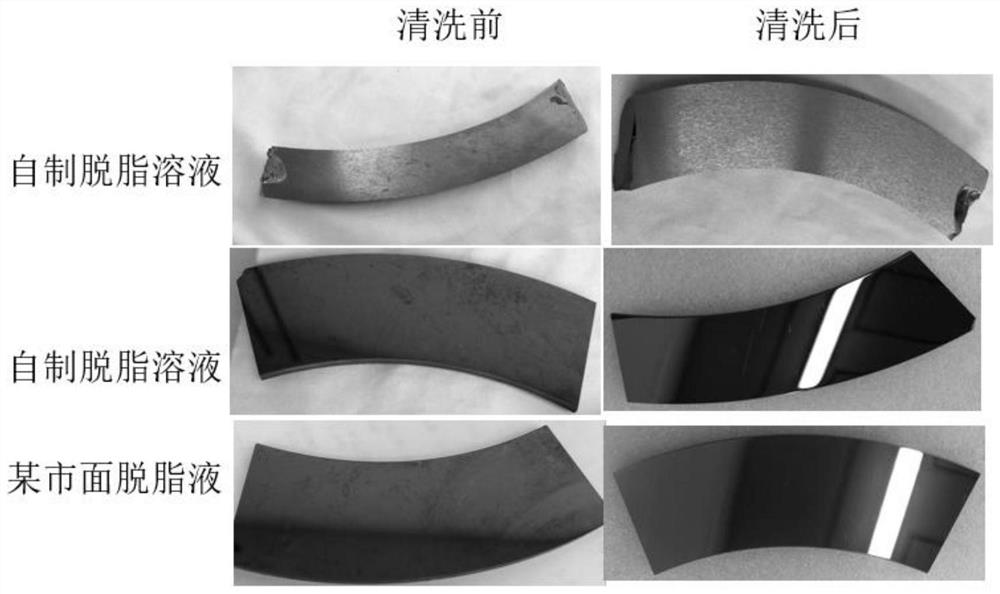
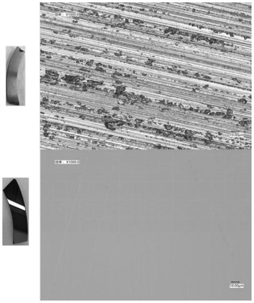
[0050] The sample after embodiment 1 and embodiment 2 degreasing treatment is detected, figure 1 It is the appearance picture of two silicon wafer samples before and after degreasing and cleaning, and the third row is the comparison picture of cleaning under the same conditions of a certain degreasing liquid on the market. It can be se...

Embodiment 3

[0053] Metal ion cleaning solution suitable for silicon, quartz, and ceramic semiconductor materials, including acidic A cleaning solution, neutral cleaning solution, and acidic B cleaning solution, which can treat the metal elements on the surface of the sample, and the metal elements include 30 elements required by the semiconductor industry Metal elements, specifically Al, Sb, As, Ba, Be, Bi, B, Cd, Ca, Cr, Co, Cu, Ga, Ge, Fe, Pb, Li, Mg, Mn, Mo, Ni, K, Na , Sr, Sn, Ti, W, V, Zn, Zr.

[0054] The sample is first soaked and cleaned with acid A lotion at room temperature. The cleaning time is about 15-20 minutes. After cleaning, it is rinsed with deionized water; Wash for about 15-20 minutes, rinse with deionized water after cleaning; finally soak in acid B lotion for cleaning, keep the temperature at room temperature, wash for about 15-20 minutes, rinse with deionized water after cleaning. Among them, the acid A lotion is: ammonium fluoride 3.9%, fluosilicic acid 2%, H-951....


PUM


Abstract

The invention relates to a cleaning method for a semiconductor material, which comprises the following specific steps of firstly, immersing the semiconductor material into an alkaline degreasing cleaning solution for degreasing treatment, and washing with deionized water after cleaning, removing metal ions, sequentially soaking and cleaning the semiconductor material with an acid A cleaning solution, and washing with deionized water after cleaning, then soaking and cleaning with neutral cleaning solution, and washing with deionized water after cleaning, and finally, soaking and cleaning in an acidic cleaning solution B, and washing with deionized water after cleaning. According to the cleaning method provided by the invention, the use concentration of strong acid is greatly reduced, and environmental pollution and corrosion to human bodies are reduced. The cleaning solution is good in stability and not prone to decomposition and volatilization, the service life of the cleaning solution is prolonged, corrosion to silicon products is small, and Ra of the washed products cannot be increased.

Description

technical field [0001] The invention belongs to the technical field of semiconductor materials, and relates to a cleaning method for semiconductor materials. Background technique [0002] In the manufacturing process of semiconductor devices such as flat panel displays such as TFT liquid crystals, micro information processors, memories, and CCDs, silicon, silicon oxide (SiO 2 ), glass, etc., on the surface of substrates such as submicron or even 1 / 4 micron for patterning or thin film formation. Therefore, in each of these manufacturing processes, the tiny contamination on the surface of the substrate must also be removed, making the surface of the substrate highly clean has become an extremely important issue; the same equipment consumables also need to be highly clean, and particulate matter is the focus of control in semiconductor engineering Objects, the products used in the project should go through the cleaning process to remove the factors that affect the particulate ...

Claims


Application Information

Patent Timeline
IPC IPC(8): H01L21/02C11D1/83C11D1/14C11D1/00C11D3/04C11D3/06C11D3/10C11D3/20C11D3/39C11D3/60C11D7/26C11D7/60
CPCH01L21/02057C11D1/83C11D3/044C11D3/06C11D3/10C11D3/2096C11D1/14C11D3/046C11D7/264C11D7/261C11D7/263C11D7/267C11D1/00C11D3/042C11D3/3942C11D3/3947C11D1/78C11D1/72C11D1/24C11D2111/22
Inventor 王燕清杨佐东
Owner 重庆臻宝实业有限公司
Why Eureka
Try Eureka