Perovskite light absorption layer and preparation method thereof, and solar cell and preparation method thereof
A solar cell and perovskite technology, applied in circuits, electrical components, electrical solid devices, etc., can solve the problems of poor reproducibility of the solution method, and the quality, consistency and work stability of the gas phase method need to be improved. The effect of quality and working stability, suppression of non-radiative recombination at the interface, and simple operation
- Summary
- Abstract
- Description
- Claims
- Application Information
AI Technical Summary
Problems solved by technology
Method used
Image
Examples
preparation example Construction
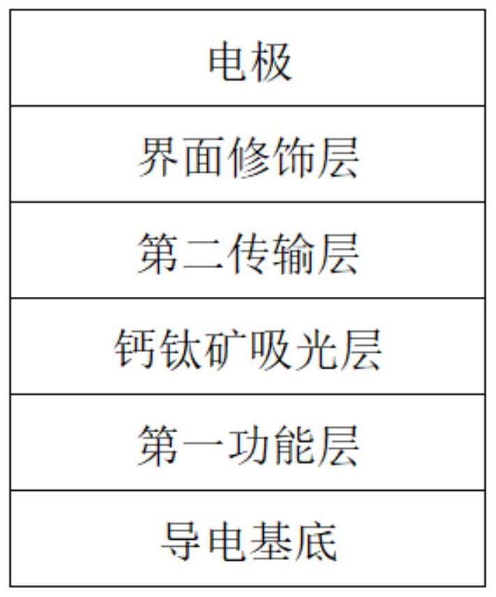
[0049] The embodiments of the present application also provide a method for preparing a perovskite light-absorbing layer, comprising the following steps:
[0050] S100: attaching the perovskite to the surface of the first functional layer to form a perovskite matrix on the surface of the first functional layer.
[0051] The first functional layer may be a hole transport layer or an electron transport layer or other functional layers, and forms a functional connection with the first functional layer.
[0052] S200: The perovskite matrix is deposited, doped and repaired with amine salt vapor to obtain a perovskite light absorbing layer.
[0053] Optionally, the reaction temperature of the deposition doping and repairing treatment is 100°C-160°C, which can keep the amine salt in a vapor state, so that the amine salt can continuously react with the perovskite matrix.
[0054] The reaction time can be adjusted according to actual needs, such as the degree of reaction, reaction r...
Embodiment 1
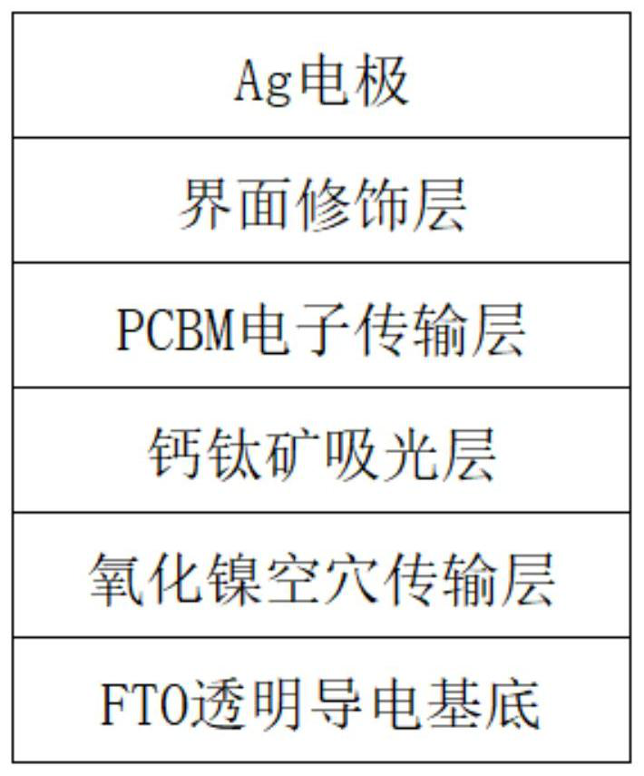
[0080] The preparation method of the solar cell of this embodiment includes the following steps:
[0081] S10: ultrasonically clean the FTO transparent conductive substrate with deionized water, acetone, isopropanol and ethanol in sequence, and then put it into an oven for drying at 70°C for later use;
[0082] S50: Ozone treatment and / or plasma cleaning are performed on the FTO transparent conductive substrate, and then a 20 nm thick nickel oxide hole transport layer is prepared by spray pyrolysis deposition on one side of the FTO transparent conductive substrate;
[0083] S60: 461mg PbI 2 Dissolve together with 159mg MAI in a mixed solvent of DMF:DMSO=2:7 (volume ratio) to prepare MAPbI with a concentration of 1.45mol / L 3 precursor fluid;
[0084] S100: The MAPbI 3 The precursor solution was spin-coated on the surface of the NiO hole transport layer by the anti-solvent method to form a thin film. Rinse the MAPbI in the spin with 400 μL anisole 10 s before the end of coat...
Embodiment 2
[0093] Except for step S200, the other steps of the solar cell preparation method in this embodiment are the same as those in Embodiment 1. S200 in this embodiment is:
[0094] MAPbI 3 The films were transferred to a tube furnace filled with MABr steam, annealed at 140 °C for 8 min, and then transferred to a glove box to cool to obtain a MABr-deposited, doped and repaired perovskite light-absorbing layer.
[0095] The photoelectric conversion efficiency of the solar cell in this embodiment is 18.6%.
PUM
 Abstract
Description
Claims
Application Information


