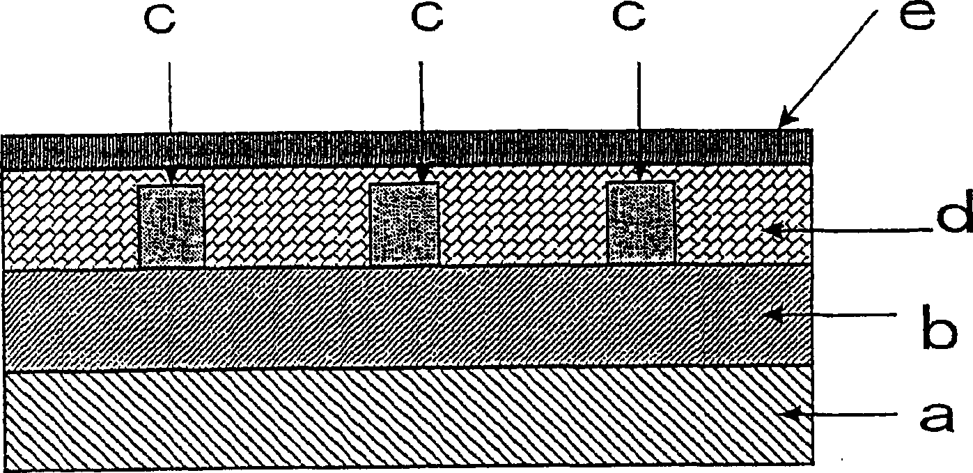
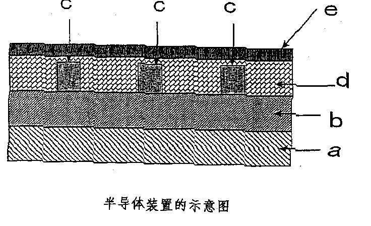
Low relative permittivity SiOx film, production method, semiconductor device using the same
A technology of relative permittivity and manufacturing method, applied in the field of low relative permittivity SiOx films, can solve the problems that semiconductor devices are difficult to achieve and the effect is only a few percent.
- Summary
- Abstract
- Description
- Claims
- Application Information
AI Technical Summary
Problems solved by technology
Method used
Image

Examples
Embodiment 1~6、 comparative example 1~4
[0099] This example is an example of using the gasification raw material bundle method.
[0100] Fully mix high-purity metal silicon powder and high-purity silicon oxide powder (ultra-differential), heat it in a graphite evaporation crucible with a high-frequency furnace to above 1800 ° C, SiOx gas, and use it together with argon as a cooling chamber, SiOx powder is recovered. The relative surface area of the SiOx powder measured by the BET method was 0 m 2 / g, and the value calculated from the analytical values of Si and oxygen was 1.2.
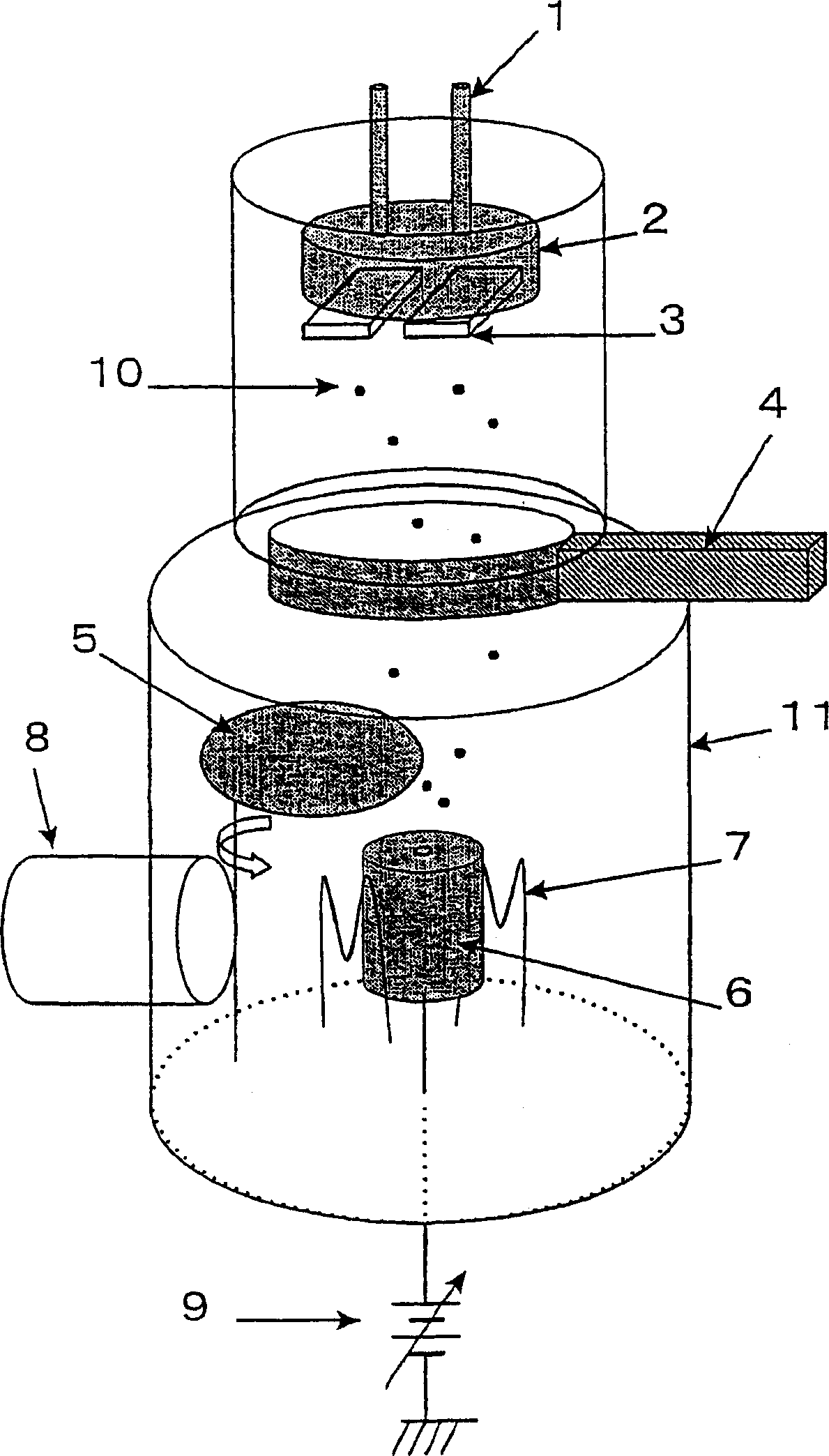
[0101] use figure 2 The SiOx powder raw material gasification raw material beam method evaporation apparatus shown in , forms a SiOx film on a single crystal silicon substrate (cooled substrate) under the conditions shown in Table 1. In the vapor deposition, a 1 / 99VOL% mixed gas of oxygen / argon flows, and by changing the flow rate, the X value of the SiOx film produced is adjusted. In addition, when the temperature of the cooling sub...
Embodiment 7~13、 comparative example 5
[0111] This example is an example using the resistance heating method.
[0112] The same SiOx powder raw material used in the above experimental example was punched to form a sample block (diameter 5mm×height 5mm). The surface area of the sample block is 80m2 / g. The relative surface area is basically the same as before forming. A SiOx film was formed on a silicon single crystal substrate having a diameter of 2 under the conditions of various gases for controlling the atmosphere and substrate temperature shown in Table 2 of this sample block in a resistance heating vapor deposition apparatus.
[0113] Also, when the temperature of the substrate is higher than room temperature, an electric heating or heater and a hot electric pan are installed behind the overtime.
[0114] The vapor deposition boat used for vapor deposition is a commercially available product made of a composite sintered body of boron nitride and titanium oxide (trade name "denka BN Composite EC" manufacture...
Embodiment 14~20
[0117] Embodiment 14~20, reference example 1,2
[0118] This example is about the modification of SiOx film.
[0119] As a SiOx powder raw material, the relative surface area of the manufacturing BET method is 110m 2 / g, X-ray diffraction is roughly amorphous, SiOx with an X value of 1.05 calculated from the analysis of silicon and oxygen, and the fluorescence X-ray analysis of the SiOx powder raw material shows that the inclusion of metal components is aluminum 200ppm, Fe100ppm, The purity of SiOx is above 99%. In addition, when the ZP binding energy of Si on carbon correction XPS was measured, it was 101.5 eV. The SiOx powder prototype was stamped with a metal film and made into a cylindrical shape with a diameter of 10mm x a height of about 10mm by CIP. The relative surface area after molding was 103M2 / g, and there was almost no change in the relative surface area before and after molding.
[0120] Put this test piece into the above-mentioned vapor deposition boat (de...
PUM
| Property | Measurement | Unit |
|---|---|---|
| relative permittivity | aaaaa | aaaaa |
| porosity | aaaaa | aaaaa |
| relative permittivity | aaaaa | aaaaa |
Abstract
Description
Claims
Application Information