Quasi-molecule laser electrochemical microstructure manufacturing method and equipment

A technology of excimer laser and manufacturing method, which can be applied to exposure devices, optics, optomechanical equipment, etc.

Inactive Publication Date: 2004-11-17
HUAZHONG UNIV OF SCI & TECH
View PDF0 Cites 7 Cited by
  • Summary
  • Abstract
  • Description
  • Claims
  • Application Information

AI Technical Summary

Problems solved by technology

However, the lasers used in the existing laser-induced electrochemical micromachining process have longer wavelengths (such as 1.06 microns or 442 nanometers) and low power (such as 4.5 milliwatts), and it is difficult for the machinable feature size to reach the submicron scale. And

Method used


Image

  • Quasi-molecule laser electrochemical microstructure manufacturing method and equipment
  • Quasi-molecule laser electrochemical microstructure manufacturing method and equipment
  • Quasi-molecule laser electrochemical microstructure manufacturing method and equipment

Examples


Embodiment 1

[0028] Embodiment 1: the processing of metal microhole array

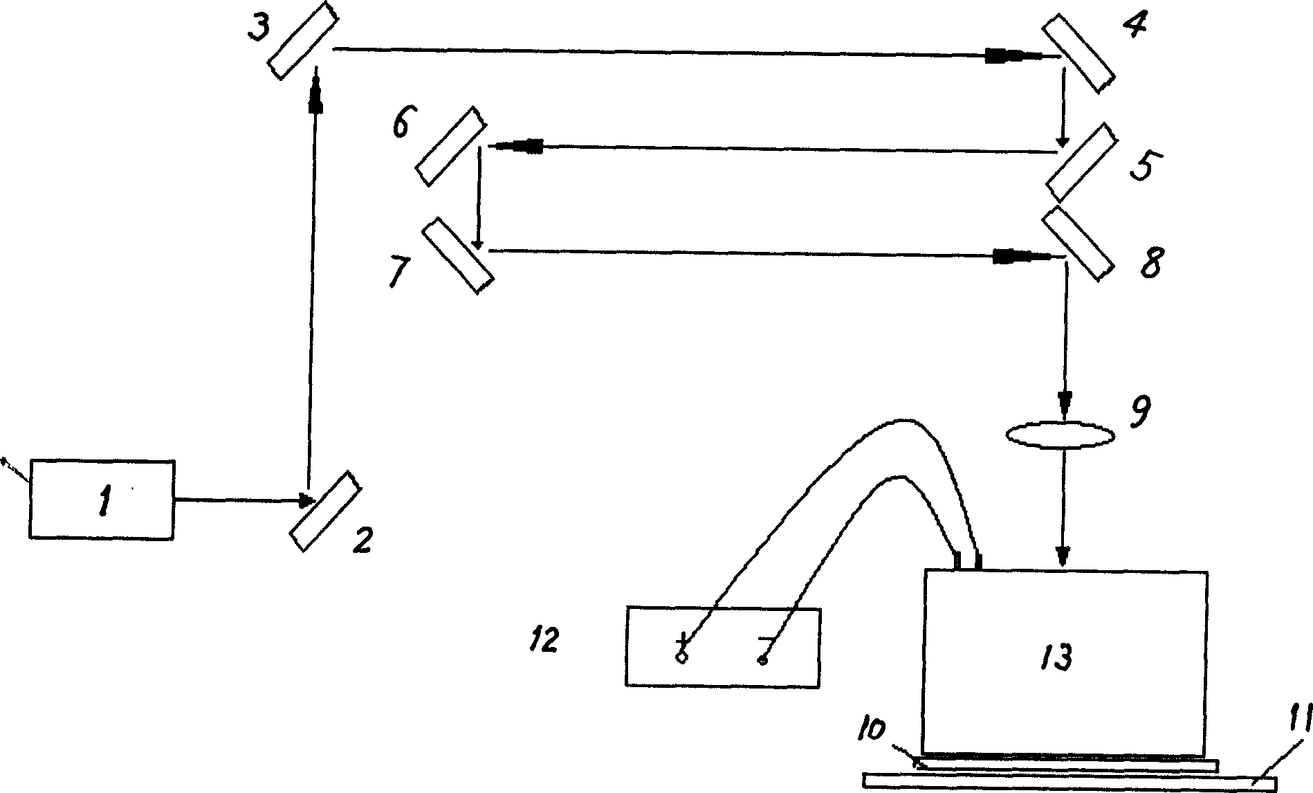
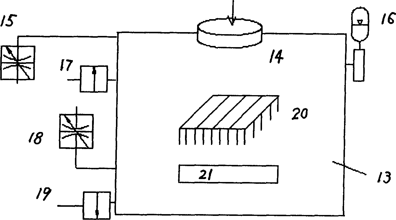
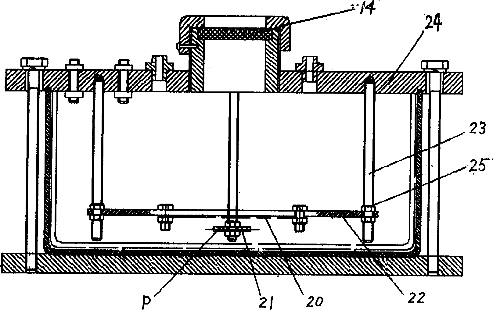
[0029] First, a layer of copper conductive layer is formed on the glass surface by chemical deposition, then, photoresist is coated on the copper conductive layer, and then the pattern is transferred to the photoresist by photolithography technology, and then it is dried. Etch and remove the photoresist, and then install the glass plate with copper conductive layer constituting the microprobe array at the cathode position in the laser electrochemical reaction chamber, so that the copper layer faces down, and connect with the cathode in it The post is connected, and the metal copper substrate to be processed is placed at the anode position, and connected to the anode terminal through the flat electrode. The distance between the electrodes is 0.2mm, the electrolyte is 5% NaCl solution, the liquid surface submerges the workpiece by 1mm, the power supply voltage is 12V, the wavelength of the excimer laser is 248nm, the...

Embodiment 2

[0030] Embodiment 2: the processing of metal microhole array

[0031] The fabrication and installation of the microprobe array are the same as the above example. The electrode spacing is 2mm, the electrolyte is 30% NaCl solution, the liquid surface submerges the workpiece by 2.5mm, the power supply voltage is 3V, the wavelength of the excimer laser is 248nm, the pulse energy is 100mJ, and the pulse number is 1000. After 1 minute, a microhole array with a pitch of 15 microns and a diameter of 5 microns is etched on the metal copper substrate with a thickness of about 0.5 mm.

Embodiment 3

[0032] Embodiment 3: the processing of metal microhole array

[0033] The fabrication and installation of the microprobe array are the same as the above example. The electrode spacing is 2mm, the electrolyte is 10% NaCl solution, the liquid surface submerges the workpiece by 2.5mm, the power supply voltage is 6V, the wavelength of the excimer laser is 248nm, the pulse energy is 250mJ, and the pulse number is 500. After 1 minute, a microhole array with a pitch of 50 microns and a diameter of 50 microns is etched on the stainless steel substrate with a thickness of about 0.5 mm.


PUM


Abstract

The invention belongs to micro manufacturing field, pointing to the deficiency of traditional method, the quasimolecule laser, integrated circuit producing and etching, electric chemical and scanning probe micro technology are integrated together into a new process method. The steps are: (1) produces micro probe array at first; (2) the base is fixed between the plane electrode and the micro probe array, generates the negative voltage, pours in the protection gas; (3) adds in voltage between the two polars after pouring the electrolyte liquid, at the same time, the quasimolecule laser are poured in to control the electrochemical reaction, completes the process. the correspondent device sets an electrochemical reaction room on the laser microprocess machine platform, it includes a laser air moving window, an inlet of protection air, a vacuum pump interface, an electrolyte liquid inlet, a microprobe array, a plane electrode, an assistant electrochemical reaction air inlet and the waste outlet. The invention can acquires microstructure with width-depth ratio 5-50, the character size 1-50 micro meter on the semiconductor base.

Description

technical field [0001] The invention belongs to the field of micro-manufacturing in manufacturing technology, and relates to integrated circuit plate-making photolithography, excimer laser processing and electrochemical processing techniques. Background technique [0002] The current micro-manufacturing method generally adopts a photolithography process to apply glue on a substrate to form a microstructure pattern, and then uses a chemical micromachining process or a laser-induced chemical micromachining process to fabricate a three-dimensional microstructure. However, since the longitudinal etching depth and lateral etching width of the microstructure formed by the chemical micromachining process are basically equal (the aspect ratio is 1), it is difficult to produce a microstructure with a large vertical depth and a small lateral width, and unnecessary "The Lateral Corrosion Problem". Laser-induced chemical micromachining can reduce harmful lateral corrosion effects and i...

Claims


Application Information

Patent Timeline
IPC IPC(8): G03F7/00G03F7/20
Inventor 史铁林陈志凌熊良才柳海鹏周月豪马龙
Owner HUAZHONG UNIV OF SCI & TECH
Why Eureka
Try Eureka