Visual temperature ladder crystal condensation growth device with low oblique and growth method thereof
A growth device and small-angle technology, which is applied in the field of crystal material growth devices, can solve problems such as lower crystal quality, lower crystal transmittance, and invisible growth process
- Summary
- Abstract
- Description
- Claims
- Application Information
AI Technical Summary
Problems solved by technology
Method used
Image
Examples
specific Embodiment approach 1
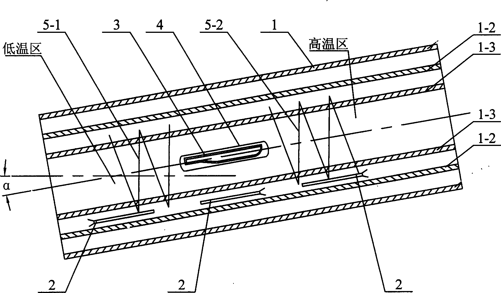
[0006] Specific embodiment 1: The device of the present invention includes a three-layer quartz tube 1, a thermocouple 2 installed between the second layer of quartz tube 1-2 and the third layer of quartz tube 1-3, and installed on the third layer of quartz tube 1. The growth boat 3 in -3, the low-temperature thermal resistance 5-1 and the high-temperature thermal resistance 5-2 installed in the second layer of quartz tube 1-2, the growth device is inclined to the ground, and the inclination angle α is 0.1-25 Degree, can be 1 degree, 3 degree, 8 degree, 10 degree, 12 degree, 18 degree, 22 degree. In the tilted device, the level of high temperature thermal resistance 5-2 is higher than that of low temperature thermal resistance 5-1 High, the outer surface of the second layer of quartz tube 1-2 is plated with gold or silver, which can keep heat and be transparent under light.
[0007] The growth method of this embodiment is as follows: the growth boat 3 containing raw materials and ...
specific Embodiment approach 2
[0008] Specific implementation manner 2: In this embodiment, the junction between the seed crystal end 3-1 and the melt end 3-2 of the growth vessel 3 is an acute angle, and the acute angle β is 1-60 degrees, which can be 5 degrees, 10 degrees, 20 degrees, 30 degrees, 40 degrees, 50 degrees.
[0009] The growth device and growth method of the present invention can be used for the growth of chalcopyrite semiconductor crystal materials. The polycrystalline raw materials are placed in a growth boat, and the growth boat materials are graphite, vitrified graphite and quartz glass coated with boron nitride coating.
[0010] Chalcopyrite semiconductor materials include IB-IIIA-VIA 2 And IIB-IVA-VA 2 Group compounds. Group IB elements include Cu, Ag, group IIIA elements include Al, Ga, In, group VIA elements include S, Se, Te; group IIB elements include Zn, Cd, Hg, group IVA elements include Si, Ge, Sn, group VA Elements include P and As.
PUM
 Abstract
Description
Claims
Application Information
 - R&D
- Intellectual Property
- Life Sciences
- Materials
- Tech Scout
- Unparalleled Data Quality
- Higher Quality Content
- 60% Fewer Hallucinations
Browse by: Latest US Patents, China's latest patents, Technical Efficacy Thesaurus, Application Domain, Technology Topic, Popular Technical Reports.
© 2025 PatSnap. All rights reserved.Legal|Privacy policy|Modern Slavery Act Transparency Statement|Sitemap|About US| Contact US: help@patsnap.com


