Wet-solid phase reaction preparation method for cadmium sulfide semiconductor nanocrystalline

A semiconductor and nanocrystal technology, applied in the field of preparation of cadmium sulfide nanocrystals, can solve the problems of different probe molecular fluorescence difficulties, difficulty in exciting multiple components at the same time, difficulty in detecting multiple components, etc., to achieve good development and Application prospect, no agglomeration phenomenon, high yield effect

Inactive Publication Date: 2005-03-16
NANJING NORMAL UNIVERSITY
View PDF0 Cites 4 Cited by
  • Summary
  • Abstract
  • Description
  • Claims
  • Application Information

AI Technical Summary

Problems solved by technology

However, if they are directly studied by fluorescence spectroscopy, the fluorescence quantum yield of bases and nucleic acids is very low, so the best way to detect them is to use various fluorescent probes
At present, the most commonly used fluorescent probes are organic dyes. In most cases, it is difficult to excite multiple components at the same time due to their narrow excitation spectrum, and their fluorescence characteristic spectrum is wide and the distribution is uneven. Symmetry, which makes it difficult to distinguish the fluorescence of different probe molecules, so it is difficult to detect multiple components at the same time
The most serious defect of organic dyes is poor photochemical stability. Photobleaching and photolysis make it impossible for each dye probe to emit too many fluorescent photons on average, and photolysis products often have a killing effect on organisms.

Method used


Image

  • Wet-solid phase reaction preparation method for cadmium sulfide semiconductor nanocrystalline
  • Wet-solid phase reaction preparation method for cadmium sulfide semiconductor nanocrystalline
  • Wet-solid phase reaction preparation method for cadmium sulfide semiconductor nanocrystalline

Examples


Embodiment 1

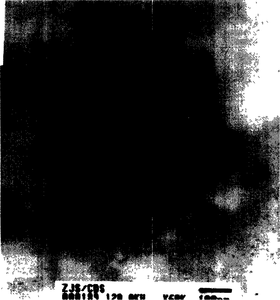
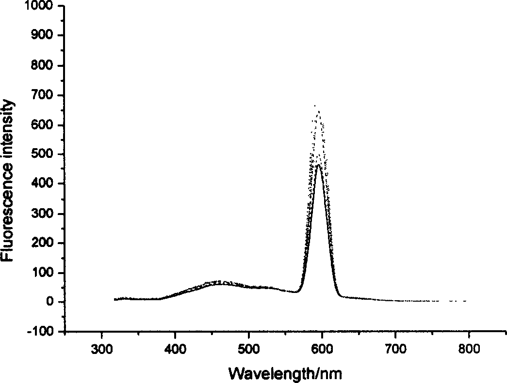
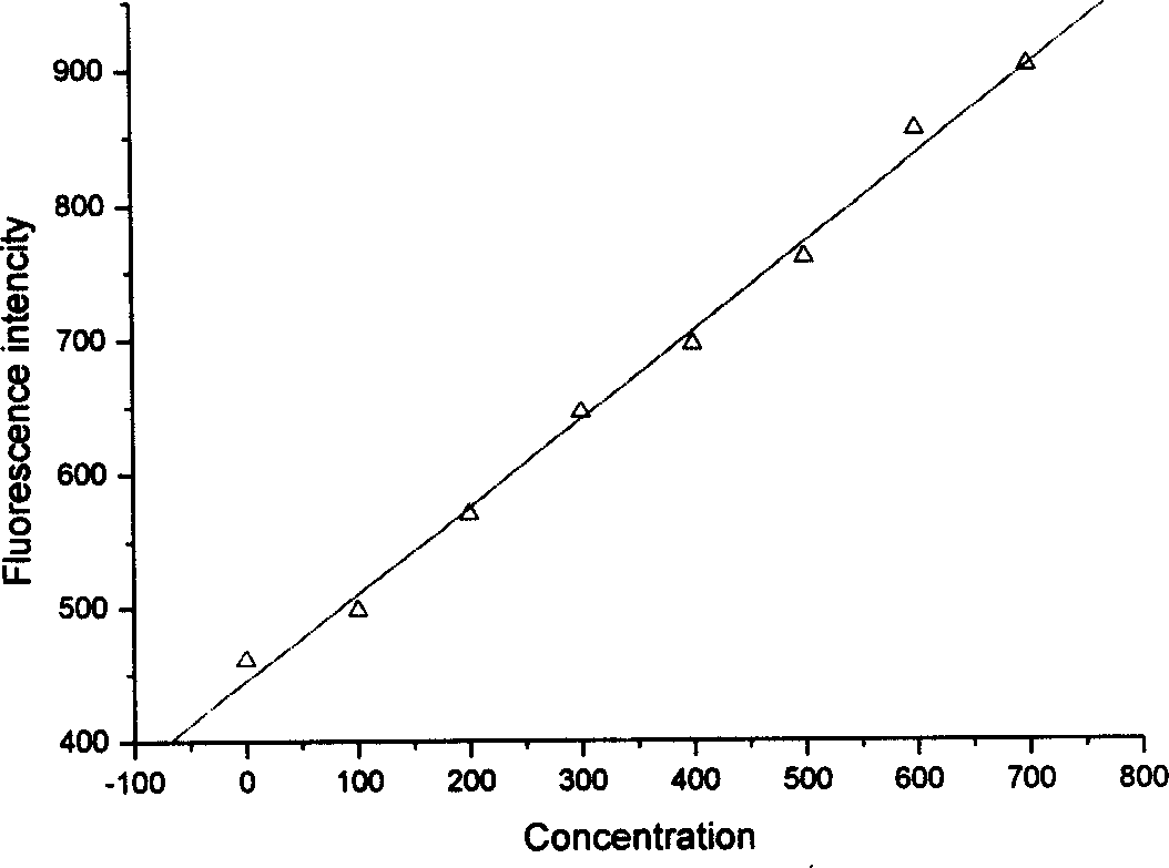
[0019] Example 1, at room temperature and under normal pressure, mix thioglycolic acid and cadmium chloride in a molar ratio of 2:1, grind in a mortar for 30 minutes, add deionized water to wash off excess thioglycolic acid, filter, and use the filter cake Wash with ionized water. Mix the filter cake and sodium sulfide in a molar ratio of 3:2, grind in an agate mortar to obtain a light yellow solid, dissolve it in water, add acetone to settle the CdS sol, filter, and wash. Vacuum dry. Get nano CdS crystals. Observed under a transmission electron microscope, the particle size of the nanoparticles is between 3-5nm, the particle distribution is uniform, and there is no agglomeration phenomenon. as attached figure 1 shown.

Embodiment 2

[0020] Embodiment 2 is substantially the same as Example 1, but the mol ratio of mercaptoacetic acid and cadmium chloride mixing is 1.8: 1; the mol ratio of filter cake and sodium sulfide is 1: 2; The solvent used for settling is ether.

Embodiment 3

[0021] Embodiment 3 is substantially the same as Example 1, but the mol ratio of mercaptoacetic acid and cadmium chloride mixing is 2.2: 1; the mol ratio of filter cake and sodium sulfide is 3.5: 2.


PUM

PropertyMeasurementUnit
particle diameteraaaaaaaaaa

Abstract

Cadmium sulfide semi-conductor nanocrystalline wet-soild phase reaction preparation method comprises the following steps : mixing thioglycolic acid with cadmium chloride according to mol raito 1.8-2.2:1, grinding, adding deionized water to scouring off excess thioglycollic acid, filtering, rinsing filter cake with deionized water, mixing filter cake and sodium sulfide according to 1-3.5:2 mol ratio, grinding, obtaining light yellow solid, dissolving the above-mentioned light yellow solid in water, adding into acetone or ether, depositing the CdS sol, filtering, rinsing, drying, obtaining nano CdS crystal. Reaction condition of the inventive is temperate, inventive process is simple, yield is high, grain size of prepared granule is uniform, not congregate. The invention has good repeatability. compared with traditional bioluminescence probe(organic dye), excitation spectrum of nano crystal is broad, and continuously distributed, while emission spectrum is symmetrically distributed and narrow, color is adjustable, which has a good application prospect in bioluminescence probe.

Description

technical field [0001] The invention relates to a method for preparing cadmium sulfide (CdS) nanocrystals, in particular to a wet-solid phase reaction preparation method for cadmium sulfide nanocrystals used as bioluminescent probes. Background technique [0002] CdS is a typical II-VI optoelectronic semiconductor material, which has a wide range of applications in light-emitting diodes, solar cells, photocatalysis, nonlinear optical materials, sensors and information storage, etc. CdS semiconductor nanomaterials have always been researched by people. hotspots. In recent years, the use of CdS semiconductor nanomaterials in biological probes has gradually attracted people's attention. At present, the preparation of CdS semiconductor nanomaterials is mainly carried out by solvothermal reaction, electrochemical deposition, sol-gel and other methods. Although these methods have their advantages, the preparation of CdS nanomaterials with good water solubility and biological mac...

Claims


Application Information

Patent Timeline
Patent Type & Authority Applications(China)
IPC IPC(8): C30B5/00C30B29/50H01S5/327H01S5/343
Inventor 张俊松李邨王炳祥余忠清
Owner NANJING NORMAL UNIVERSITY
Why Eureka
Try Eureka