Printed wiring board for semiconductor plastic package

a technology of printed wiring and plastic packaging, which is applied in the direction of transportation and packaging, sustainable manufacturing/processing, and final product manufacturing. it can solve the problems of reduced size of solder ball pads, defective products, and heat resistance of substrates and electric insulation of multi-layers

Inactive Publication Date: 2002-04-04
MITSUBISHI GAS CHEM CO INC
View PDF0 Cites 14 Cited by
  • Summary
  • Abstract
  • Description
  • Claims
  • Application Information

AI Technical Summary

Benefits of technology

[0006] It is another object of the present invention to provide a printed wiring board for a CSP in which the distortion of the printed wiring board is decreased and the distortion of a semiconductor plastic package formed by mounting a semiconductor chip on the printed wiring board by wire bonding or flip chip bonding is decreased.
[0007] It is further another object of the present invention to provide a printed wiring board for a CSP, which overcomes the degradation of heat resistance, electric insulation after water absorption and anti-migration properties, which degradation is caused by a decrease in the thickness, size and weight of packages.
[0019] According to the present invention, there is provided a printed wiring board for a CSP, which is excellent in the adhesion of solder balls to a substrate, and further, which is excellent in properties such as heat resistance, electric insulation after water absorption and anti-migration properties due to the use of the above-described resin.

Problems solved by technology

The above tendency causes problems on heat resistance of a substrate and electric insulation of a multi-layered board after water absorption and anti-migration properties.
In a conventional plastic ball grid array (P-BGA) and CSP, the adhesion of solder balls to a base material decreases with a decrease in the size of a solder ball pad, which causes defective products.
Further, since a substrate has a small thickness, a printed wiring board inevitably undergoes distortion due to a variability of thickness of solder resists on front and reverse surfaces of a substrate and a difference in residual ratios of copper foils.
Undesirably, therefore, the use of an organic solvent is troublesome in view of processing, and further, a contamination problem in a post-step is caused.
However, when it is poor in workability and economic performances, etc., due to its low curing rate, a known heat-curing catalyst is incorporated into the thermosetting resin.
A powder containing Na, K or Cl ion is not preferred since it has a detrimental effect on the reliability of a semiconductor.
It is therefore poor in workability as a printed wiring board and it has a high defect ratio.

Method used


Image

  • Printed wiring board for semiconductor plastic package
  • Printed wiring board for semiconductor plastic package
  • Printed wiring board for semiconductor plastic package

Examples


example 1

[0067] 900 Parts of 2,2-bis(4-cyanatophenyl)propane and 100 parts of bis(4-maleimidophenyl)methane were melted to 150.degree. C. and allowed to react for 4 hours with stirring, to give a prepolymer. The prepolymer was dissolved in mixed solvents of methyl ethyl ketone and dimethylformamide. To the resultant mixture were added 400 parts of a bisphenol A type epoxy resin (trade name: Epikote 1001, supplied by Yuka-Shell Epoxy K.K.) and 600 parts of a cresol novolak type epoxy resin (trade name: ESCN-220F, supplied by Sumitomo Chemical Industry Co., Ltd.), and these materials were homogeneously dissolved and mixed. Further, as a catalyst, 0.4 part of zinc octylate was added, dissolved and mixed. To the resultant mixture were added 500 parts of an inorganic filler (trade name: Calcined Talc BST #200, supplied by Nippon Talc K.K.) and 8 parts of a black pigment, and these materials were homogeneously stirred and mixed to prepare a varnish A. A 50 .mu.m thick glass woven fabric having a w...

example 2

[0069] 700 Parts of an epoxy resin. (trade name: Epikote 5045), 300 parts of an epoxy resin (trade name: ESCN-220F), 35 parts of dicyandiamide and 1 part of 2-ethyl-4-methylimidazole were dissolved in mixed solvents of methyl ethyl ketone and dimethyl formamide, and the mixture was homogeneously stirred. The same glass fabric as that used in Example 1 was impregnated with the above mixture, and the impregnated glass fabric was dried to give a prepreg E having a gelation time of 150 seconds.

[0070] Three sheets of the above prepreg E were combined, and 12 .mu.m thick electrolytic copper foils were placed on both the surfaces of the combined sheets, one on one surface and one on the other surface. The resultant set was laminate-formed at 190.degree. C. at 20 kgf / cm.sup.2 under a vacuum of 30 mmHg or less to give a double-side copper-clad laminate having a thickness of 189 .mu.m which includes the thickness of the copper foil. Three blind holes having a diameter of 125 .mu.m each were s...

example 3

[0081] The same varnish A as that used in Example 1 was prepared, and a varnish F was prepared in the same manner as in Example 1 except that the addition of 500 parts of the inorganic filler and 8 parts of the black pigment was omitted.

[0082] A 50 .mu.m thick glass woven fabric (weight: 53 g / m.sup.2, gas permeability: 7 cm.sup.3 / cm.sup.2.sec) was impregnated with the varnish A and the impregnated glass woven fabric was dried at 150.degree. C. to obtain a prepreg G1 having a gelation time 120 seconds (at 170.degree. C.) and having a resin composition content of 51% by weight or a prepreg G2 having a gelation time of 103 seconds and having a resin composition content of 60% by weight.

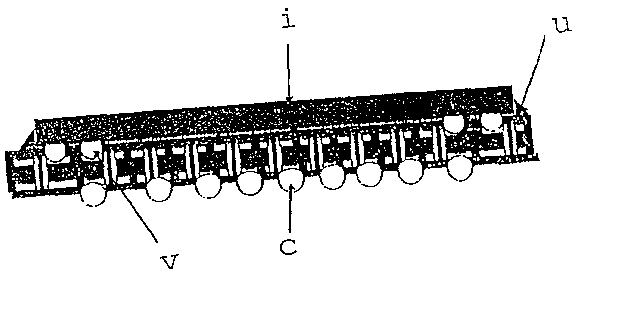
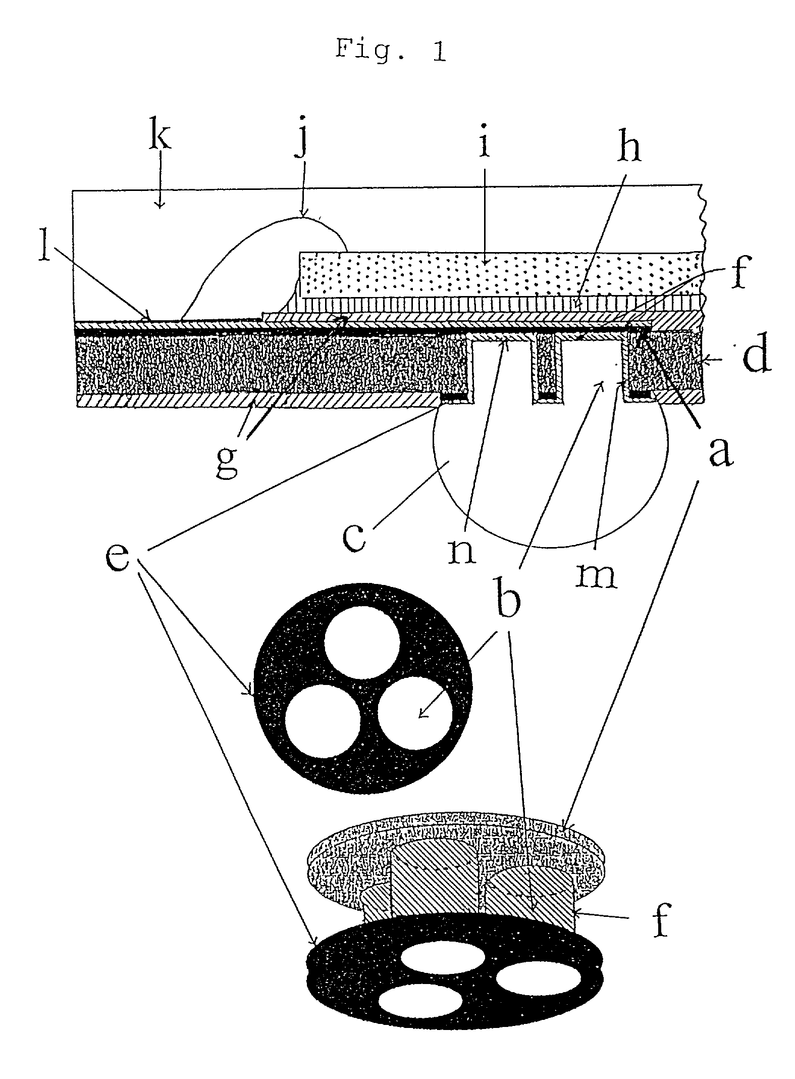
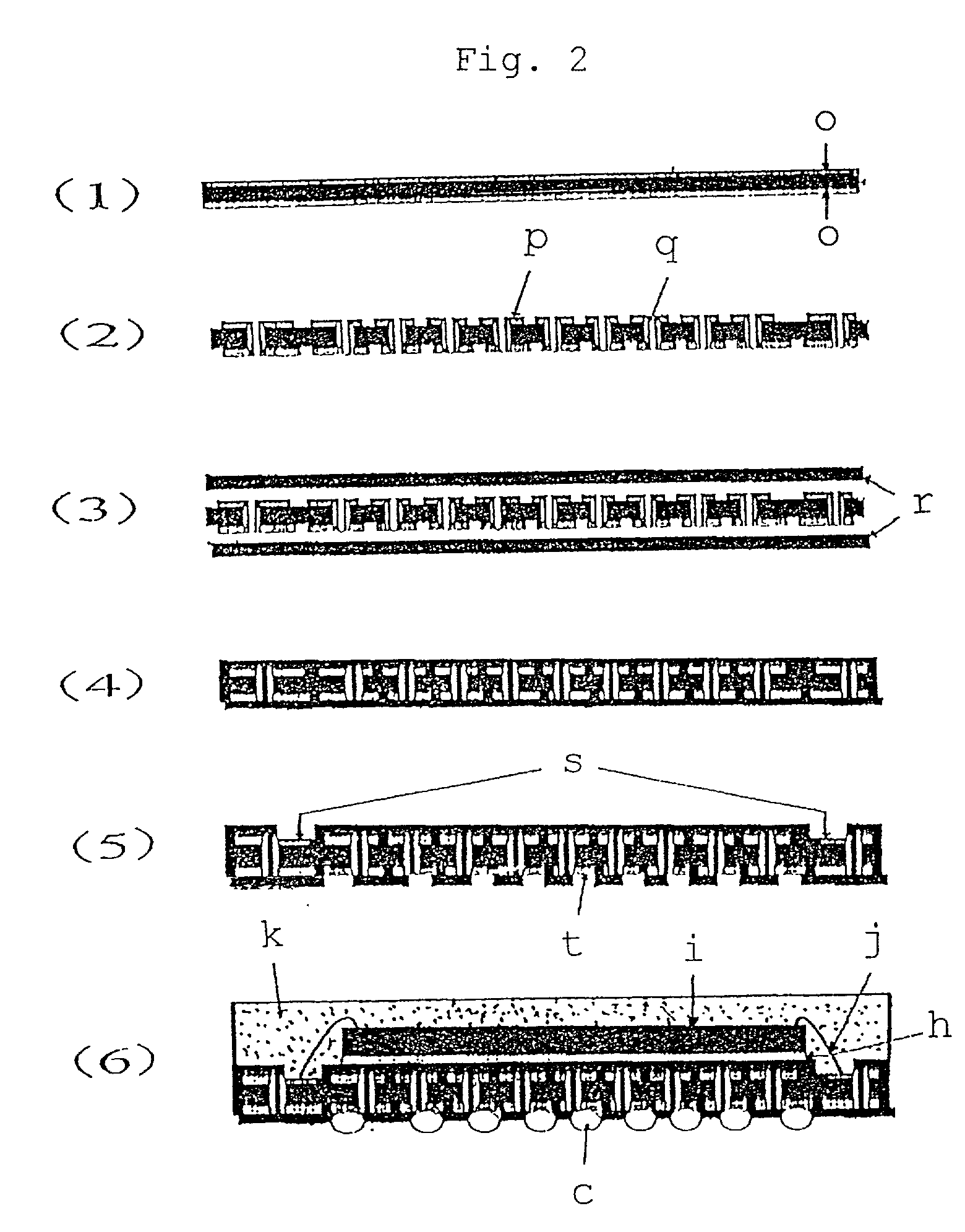
[0083] Electrolytic copper foils (o in FIG. 2) having a thickness of 12 .mu.m each were placed on both the surfaces of combined two sheets of the prepreg G1, and the resultant set was laminate-formed at 200.degree. C. at 20 kgf / cm.sup.2 under a vacuum of 30 mmHg or lower for 2 hours, to give a double-sid...


PUM

PropertyMeasurementUnit
thicknessaaaaaaaaaa
bond energyaaaaaaaaaa
melting pointaaaaaaaaaa

Abstract

Provided is a printed wiring board for a chip size scale package, which overcomes the poor adhesion of solder balls to a base material which poor adhesion is caused by a recent decrease in the size of the solder balls, and in the chip size scale package, the distortion of the printed wiring board is decreased and the distortion of a semiconductor plastic package formed by mounting a semiconductor chip on the printed wiring board by wire bonding or flip chip bonding is decreased. The printed wiring board has, as a substrate for a chip scale package, a double-side copper-clad laminate formed of an insulation layer and having copper foils on both surfaces, wherein the double-side copper-clad laminate has an upper copper foil surface and a lower copper foil surface, the upper copper foil surface has a wire bonding or flip chip bonding terminal and has a copper pad in a position where the copper pad can be electrically connected to said wire bonding or flip chip bonding terminal and can be connected to a blind via hole formed in the lower copper surface, the lower copper foil surface has a solder-balls-fixing pad in a position corresponding to said copper pad, the solder-balls-fixing pad has at least 2 blind via holes within itself, and the solder-balls-fixing pad connected to a reverse surface of the copper pad with a conductive material is electrically connected with solder balls which are melted and filled in blind via holes so as to be mounded.

Description

[0001] The present invention relates to a printed wiring board for a semiconductor plastic package. More specifically, it relates to a printed wiring board for a chip scale package (CSP) formed of a semiconductor chip mounted on a small-sized printed wiring board having almost the same size as the semiconductor chip, and particularly, it relates to a printed wiring board for a very thin ball grid array (BGA) type plastic package.[0002] The printed wiring board as an end product of the present invention, with a semiconductor chip on it, is used in / as a micro-controller, an application specific IC (ASIC), a memory, or the like. The above package is connected to a mother board printed wiring board with solder balls and used in an electronic machine or equipment.DESCRIPTION OF PRIOR ART[0003] A conventional base material for the chip scale package (CSP) is mainly selected from thin sheets formed of a glass epoxy material, a polyimide film material and a ceramic material. In packages for...

Claims


Application Information

Patent Timeline
Patent Type & Authority Applications(United States)
IPC IPC(8): H01L23/498H05K1/03H01L21/60H05K1/11H05K3/00H05K3/34
CPCH01L23/13H01L23/49811H01L23/49816H01L23/49866H01L24/45H01L2224/0401H01L2224/05647H01L2224/131H01L2224/16225H01L2224/32225H01L2224/45H01L2224/48091H01L2224/48227H01L2224/48228H01L2224/73265H01L2924/01006H01L2924/01012H01L2924/01013H01L2924/01014H01L2924/01025H01L2924/01028H01L2924/01029H01L2924/0103H01L2924/01033H01L2924/01046H01L2924/01047H01L2924/0105H01L2924/01051H01L2924/01056H01L2924/01078H01L2924/01079H01L2924/01083H01L2924/01105H01L2924/04941H01L2924/15311H05K1/0373H05K1/112H05K3/0038H05K3/3436H05K3/4629H05K2201/0209H05K2201/09472H05K2201/09509H05K2201/0979H01L24/48H01L2224/73204H01L2924/01005H01L2924/01019H01L2924/01023H01L2924/01042H01L2924/01045H01L2924/01074H01L2924/014H01L2924/40252H01L2924/01015Y10T428/24917H01L2924/00014H01L2924/00012H01L2924/00H01L2924/0002H01L2924/12042H01L24/73H01L2924/181Y10T428/31681Y02P70/50H01L2224/45099H01L2224/43H01L21/60
Inventor KIMBARA, HIDENORIIKEGUCHI, NOBUYUKIKOMATSU, KATSUJI
Owner MITSUBISHI GAS CHEM CO INC
Why Eureka
Try Eureka