

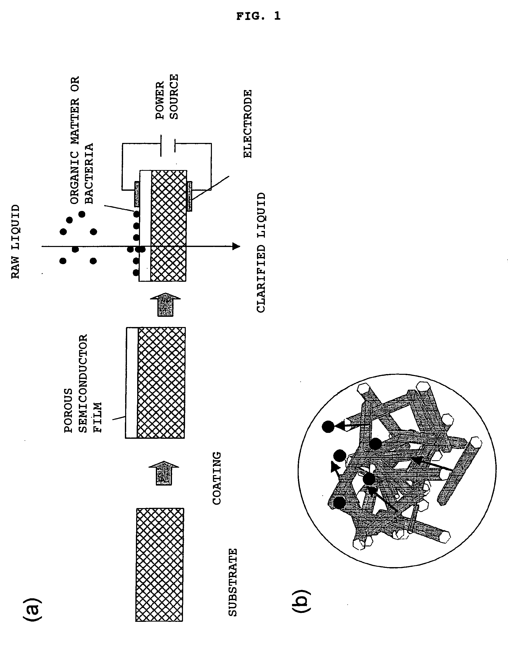
Porous semiconductor and process for producing the same
a technology of porous semiconductors and semiconductors, applied in the field of porous semiconductors, can solve the problems of weak effect, serious obstacle to their practical application, and increase the cost, and achieve the effects of low cost, high luminance, and easy manufacturing
- Summary
- Abstract
- Description
- Claims
- Application Information
AI Technical Summary
Benefits of technology
Problems solved by technology
Method used
Image

Examples
example 1
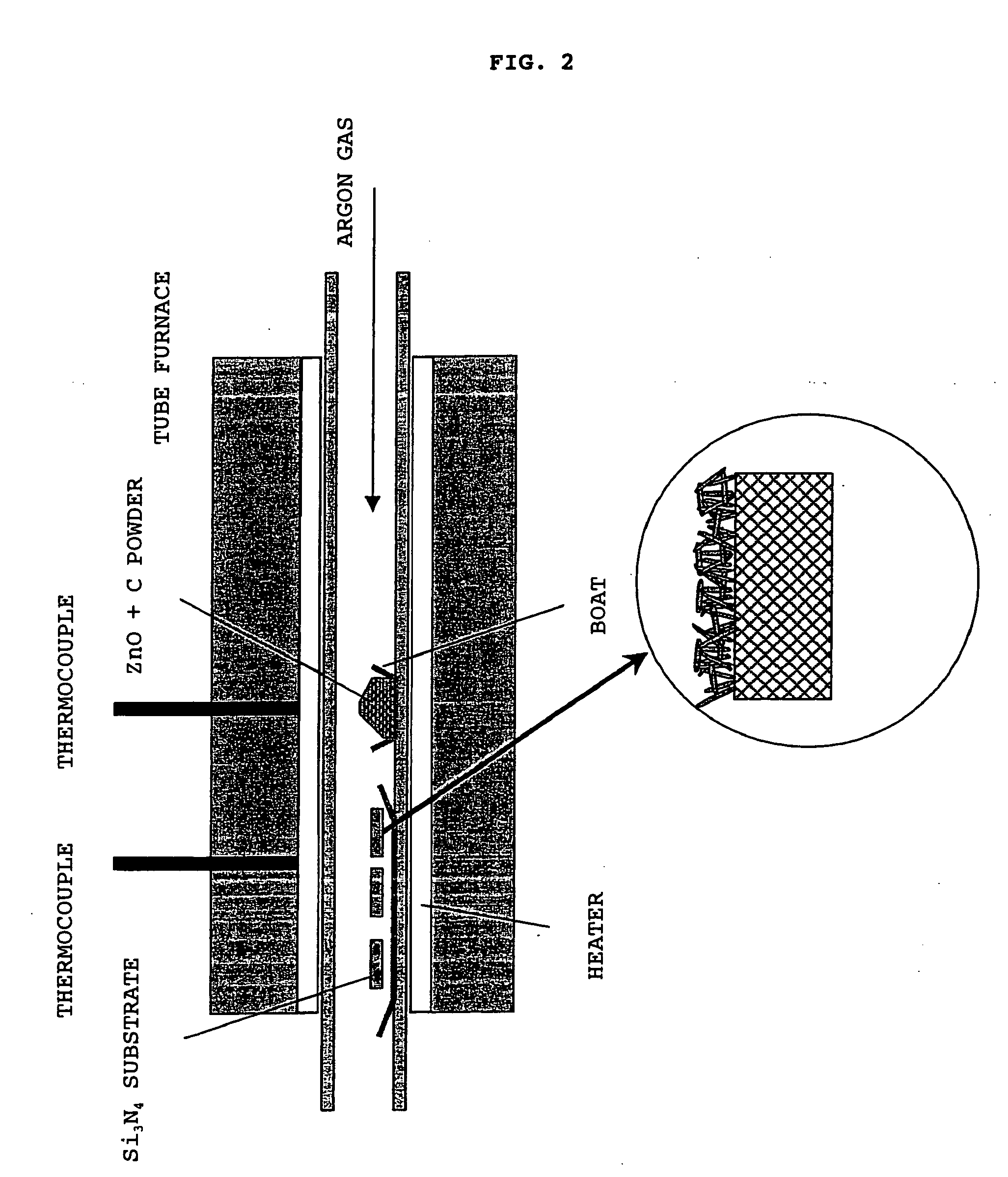
[0257] A substrate was produced by sputtering a 50 Å coating of gold onto a porous plate of SUS316 with a diameter of 25 mm and a thickness of 1 mm. The substrate had a porosity of 50% and a pore size of 10 μm diameter. A mixture of graphite powder and ZnO powder with an average particle size of 1 μm diameter was placed in an aluminum boat, and this was inserted along with the substrate into a tube furnace held at a temperature of 925° C. under an argon gas flow at atmospheric pressure, and heated for 30 minutes. The raw material powder was placed at the center of the furnace tube, while the substrate was placed downstream from the center where the temperature was kept somewhat lower.
[0258] Whiskers were produced on the surface of the heated substrate. X-ray analysis revealed the whiskers to be ZnO. The following Samples 1 and 2 were produced from the obtained sample.
[0259] Sample 1: An electrode was formed on the substrate surface and the surface of the whiskers of the sample.
[0...
example 2
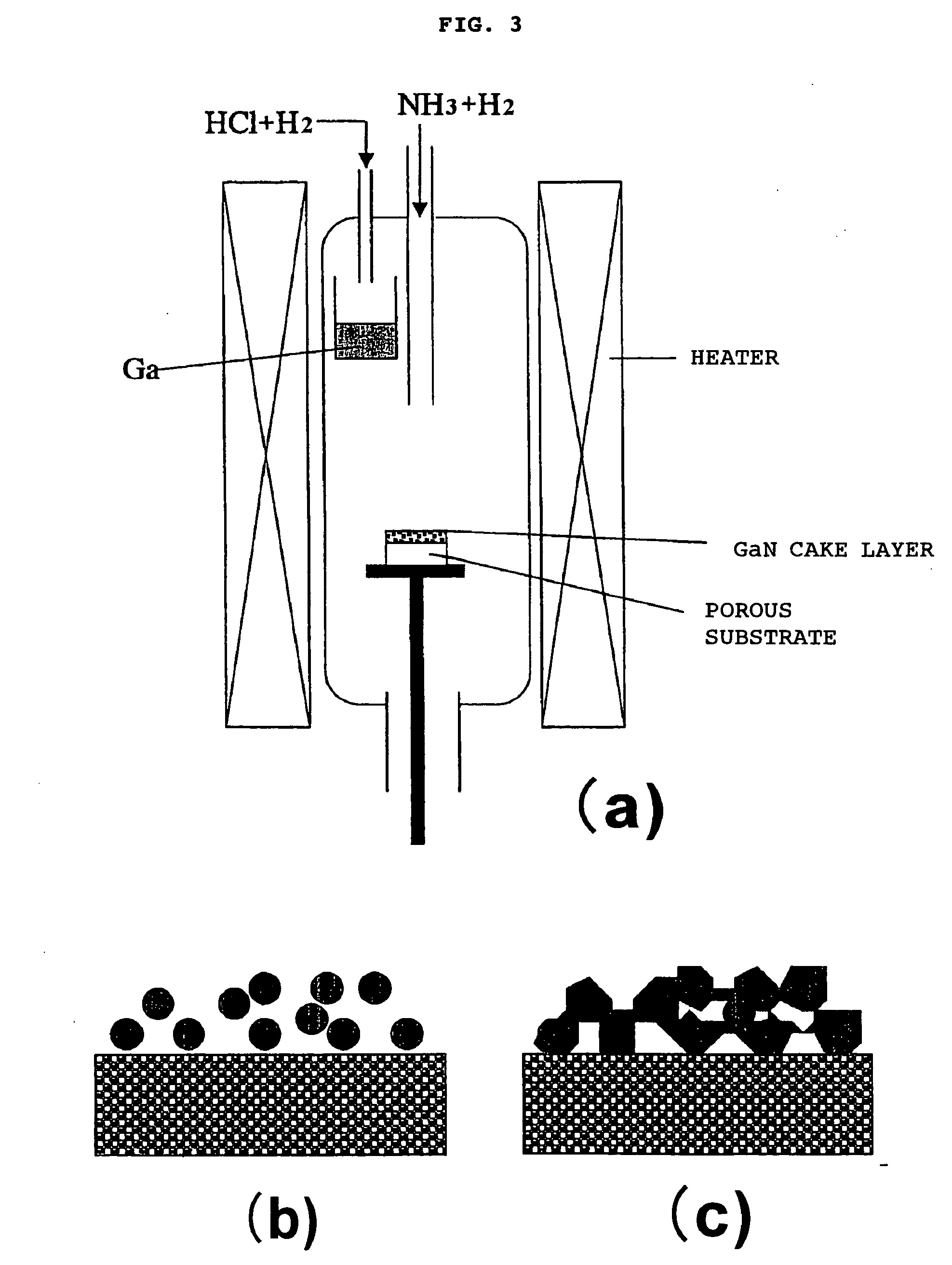
[0266] Porous SiC with a diameter of 25 mm and a thickness of 1 mm was used as the substrate. The porosity was 50% and the pore size was 10 μm. As shown in FIG. 4, AlN powder (with a purity of 99.99%, containing 0.01% magnesium as an impurity) packed in a crucible and a porous SiC substrate were placed a super-high-temperature furnace. The pressure inside the furnace was lowered to close to a vacuum, after which the raw material area was heated to between 2000 and 2200° C., and the substrate area to 1900° C. N2 was then introduced and the pressure inside the furnace was held at 40 kPa. This state was maintained for 2 hours, after which the system was cooled to room temperature.
[0267] Whiskers were produced on the surface of the heated substrate. X-ray analysis revealed the whiskers to be AlN. The product of forming an electrode on the substrate surface and the surface of the whiskers of the sample obtained when the temperature in the raw material area was 2200° C. was termed “Sampl...
example 3
[0274] Porous SUS316 with a diameter of 25 mm and a thickness of 1 mm was used as the substrate. The porosity was 40% and the pore size was 3 μm. As shown in FIG. 11, a mixture of graphite powder and Ga2O3 powder with an average particle size of 1 μm was placed in an aluminum boat, and this was inserted along with the substrate into a tube furnace held at a temperature of 900° C. under an NH3—N2—H2 gas flow, and heated for 1 hour. The raw material powder was placed at the center of the furnace tube, while the substrate was placed downstream where the temperature was kept at 650° C., which is lower than that of the center. Whiskers were produced on the surface of the heated substrate. X-ray analysis revealed the whiskers to be GaN.
[0275] The following Samples 5 and 6 were produced from the obtained sample.
[0276] Sample 5: An electrode was formed on the substrate surface and the surface of the whiskers of the sample.
[0277] Sample 6: Titanium isopropoxide (Ti(OC2H5)4), which is an a...
PUM
| Property | Measurement | Unit |
|---|---|---|
| Size | aaaaa | aaaaa |
| Wavelength | aaaaa | aaaaa |
| Wavelength | aaaaa | aaaaa |
Abstract
Description
Claims
Application Information