Trench capacitor with insulating collar, and appropriate method of fabrication

a technology of insulating collar and clamping capacitor, which is applied in the direction of semiconductor devices, electrical equipment, transistors, etc., can solve the problems of low storage capacity, affecting the operability and usability of memory equipment, and the ratio may be too small to produce an adequate signal, so as to reduce the parasitic capacitance of the space-charge zone, increase the complexity of production, and reduce the resistance of the electrod

Inactive Publication Date: 2005-08-11
INFINEON TECH AG
View PDF5 Cites 9 Cited by
  • Summary
  • Abstract
  • Description
  • Claims
  • Application Information

AI Technical Summary

Benefits of technology

[0025] One advantage of the present invention is that the electrode resistance can be reduced without increasing the complexity of production. By using low-resistance metal electrodes, the parasitic capacitance of the space-charge zone can be eliminated.
[0026] Special metal electrode materials which are proposed are materials from the class including metal borides, metal phosphides and metal antimonides. Specifically, the borides, phosphides and antimonides of the transition metals from the secondary groups IV, V and VI of the periodic table are proposed (particularly titanium, zirconium, hafnium, vanadium, niobium, tantalum, chromium, molybdenum, tungsten).
[0027] These are distinguished not only by mechanical hardness and chemical resistance, but also by high thermal stability (melting points in some cases greater than 2500° C.), even in contact with s...

Problems solved by technology

However, the use of smaller capacitors results in a lower storage capacity, which in turn can adversely affect the operability and usability of the memory apparatus.
If the ...

Method used


Image

  • Trench capacitor with insulating collar, and appropriate method of fabrication
  • Trench capacitor with insulating collar, and appropriate method of fabrication
  • Trench capacitor with insulating collar, and appropriate method of fabrication

Examples


first embodiment

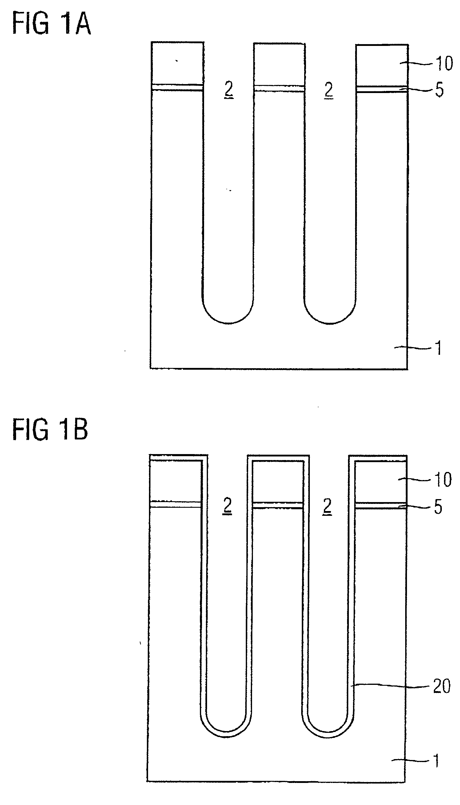
[0045] In the case of the present first embodiment, a pad oxide layer 5 and a padnitride layer 10 are first of all deposited on a silicon substrate 1, as shown in FIG. 1a. Next, a further oxide layer (not shown) is deposited and these layers are then patterned using a photoresist mask (likewise not shown) and an appropriate etching method to form a “hard mask”. Using this hard mask, trenches 2 with a typical depth of approximately 1-10 μm are etched into the silicon substrate 1. The topmost oxide layer is then removed in order to arrive at the state shown in FIG. 1a.

[0046] In a subsequent process step, as FIG. 1b shows, arsenic silicate glass (ASG) 20 is deposited on the resultant feature, so that the ASG 20 fully lines the trenches 2, in particular.

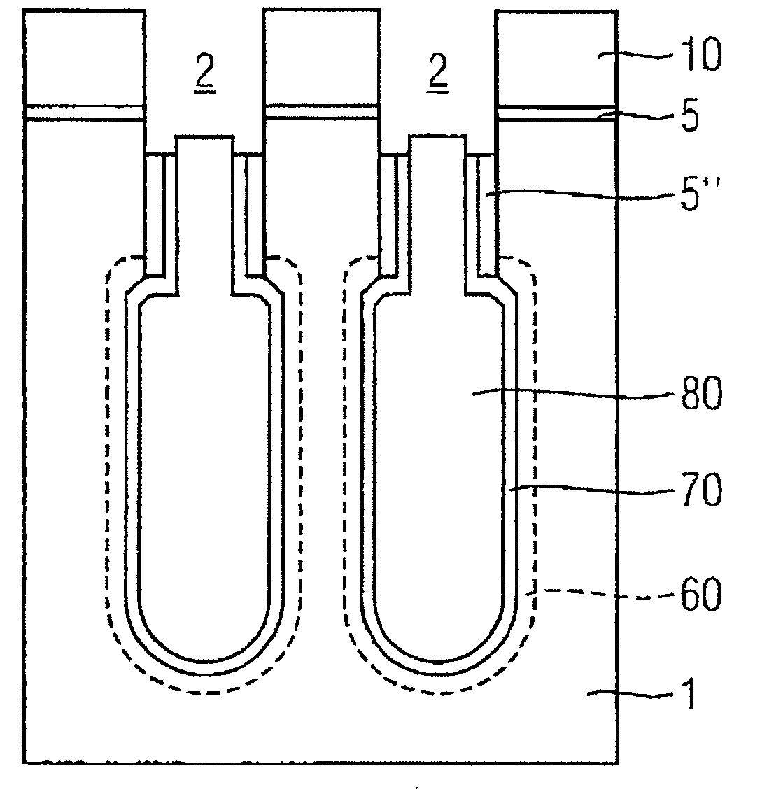
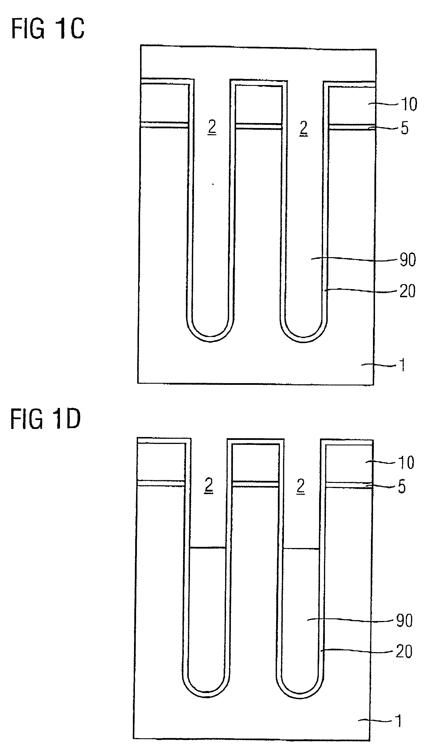
[0047] As FIG. 1c shows, the deposition of the ASG layer 20 is followed by the resultant feature being filled with undoped polycrystalline silicon 90, which is subsequently removed by isotropic dry-chemical etching in the upper region ...

second embodiment

[0063] The state shown in FIG. 2a corresponds to the state shown in FIG. 1j, whose previous history has been explained in detail above in connection with the

[0064] In line with FIG. 2b, a film 100 made of a special metal electrode material is subsequently provided, specifically a TiN / TiP stack. This means that there is the advantage of the thermal stability of TiN and the very good conductivity of TiP, for example.

[0065] In this connection, R. Leutenecker et al. describe, in “Microelectronic Engineering”, 37 / 38, pages 397 ff., 1997, deposition of TiN using a CVD method and subsequent annealing of the TiN layer in phosphine at 450° C., forming an upper layer made of titanium phosphide.

[0066] In the next process step, arsenic-doped polysilicon 80 or polysilicon germanium is deposited, which results in the feature shown in FIG. 2c.

[0067] By etching back the polysilicon or polysilicon germanium 80, the feature shown in FIG. 2d is obtained.

[0068] Finally, the metal electrode film 100...


PUM


Abstract

The present invention provides a trench capacitor, particularly for use in a semiconductor memory cell, having a trench which is formed in a semiconductor substrate; a first conductive capacitor plate which is situated in and/or next to the trench; a second conductive capacitor plate which is situated in the trench; a dielectric layer, which is situated between the first and second capacitor plates, as capacitor dielectric; and an insulating collar in the upper region of the trench. At least one layer of the first first conductive capacitor plate and/or of the second conductive capacitor plate is made of a material from the class containing the metal borides, metal phosphides and metal antimonides of the transition metals from the secondary groups IV, V and VI of the periodic table.

Description

CLAIM FOR PRIORITY [0001] This application claims the benefit of priority to German Application No. 10 2004 005 694.3 which was filed in the German language on Feb. 5, 2004, the contents of which are hereby incorporated by reference. TECHNICAL FIELD OF THE INVENTION [0002] The present invention relates to a trench capacitor, particularly for use in a semiconductor memory cell, having a trench which is formed in a semiconductor substrate, and to a method of fabrication. BACKGROUND OF THE INVENTION [0003] Although they may be applied to any trench capacitors, the present invention and the problems on which it is based are explained below with reference to a trench capacitor used in a DRAM memory cell. Such memory cells are used in integrated circuits (ICs), such as random access memories (RAMs), dynamic RAMs (DRAMs), synchronous DRAMs (SDRAMs), static RAMs (SRAMs) and read-only memories (ROMs). Other integrated circuits contain logic apparatuses, such as programmable logic arrays (PLA...

Claims


Application Information

Patent Timeline
IPC IPC(8): H01L21/334H01L21/822H01L21/8242H01L27/08H01L27/108H01L29/76H01L29/94H01L31/119
CPCH01L27/10861H01L29/945H01L29/66181H01L27/1087H10B12/038H10B12/0387
Inventor SEIDL, HARALD
Owner INFINEON TECH AG
Why Eureka
Try Eureka