
Flexible printed circuit board and process for producing the same

a printed circuit board and flexible technology, applied in the direction of insulating substrate metal adhesion improvement, conductive layers on insulating supports, applications, etc., can solve the problems of reducing the dimensional accuracy and electrical characteristics of the adhesive, the need for lightweight and highly functional design has not yet been satisfied sufficiently, and the conventional film has problems to be solved

Inactive Publication Date: 2005-08-11
PANASONIC CORP
View PDF1 Cites 13 Cited by
  • Summary
  • Abstract
  • Description
  • Claims
  • Application Information

AI Technical Summary

Benefits of technology

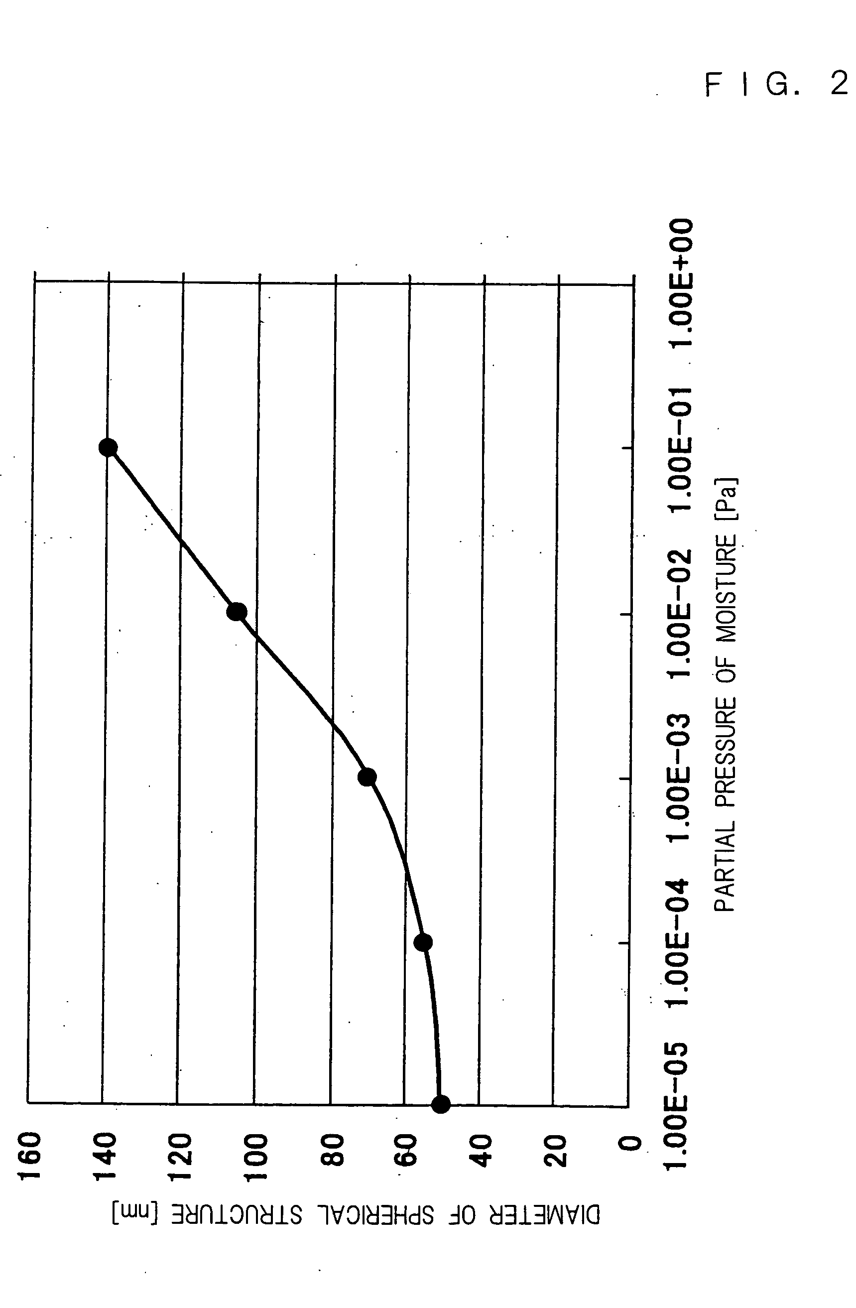
[0057] (23) In the method for producing the flexible printed circuit board in accordance with the present invention, it is preferable that the step of subjecting the plastic film substrate to dewatering processing in vacuum includes a step of carrying out dewatering processing so that the partial pressure of moisture is 10−3 Pa or less.

Problems solved by technology

In a conventional film obtained by bonding copper foil to a plastic film, the need for high-density thin-line design is satisfied by improving the heat resistance of adhesive and by making the copper foil thinner; however, the need for lightweight and highly functional design has not yet been satisfied sufficiently.
In addition, the conventional film has problems to be solved, such as reduction in dimensional accuracy and reduction in electrical characteristics owing to the use of adhesive.
Furthermore, in a method for forming very fine circuit patterns having a thickness of 10 μm or less, the handling in a step of bonding the very fine circuit patterns to a film substrate is particularly difficult, thereby causing problems, such as the generation of creases and the adhesion of impurities.
However, these film forming methods have problems; long time is required to form a necessary thickness of 5 to 10 μm, and the adhesion strength between the plastic film substrate and the copper thin film is insufficient.
However, this evaporation plating method requires acid processing during plating processing, thereby causing a problem of delaminating an evaporated film during this acid processing.
However, in the case when the printed circuit board is left stationary in an environment of supersaturated steam of 120° C. at 2 atm after being subjected to electrolytic copper plating, there is a problem of being unable to maintain its desired peeling strength.
In addition, in this production method, a step of forming a metal film serving as the intermediate layer 12 is necessary; for this purpose, etching processing and dewatering processing are required to be carried out, thereby having a problem of increasing cost.
However, this method has problems; insulation performance reduces since tin is present in the polyimide film, and etching efficiency lowers since an anchor evaporation layer for copper evaporation is required.
Furthermore, this method also has problems to be solved; cost for forming a film of a chromium-based alloy and cost for dewatering processing are required, and environmental loads are large.
However, the kinetic energy of the copper atom in sputtering is 5 eV at most (50 eV at a maximum), and the peeling strength has fluctuations depending on the surface state of the plastic film, thereby causing a problem of being unable to obtain a peeling strength of 1 kg / cm, the target of the product.
Hei 5-251511, the peeling strength of the copper thin film has fluctuations and does not satisfy a desired strength in some cases.
In addition, in the disclosed production method, the plasma processing is carried out by using a reactive ion etching apparatus; however, in this kind of production method, the kinetic energy of ionized nitrogen plasma is 5 eV to 10 eV at most, whereby the generation of the functional groups is insufficient.
Furthermore, since the kinetic energy in this production method is low, the generation of functional groups is greatly depending on the surface state of the plastic film, thereby causing a problem of being unable to securely generate functional groups on the plastic film.
However, the specific conditions of forming a metal thin film on a plastic film, the relationship in peeling strength between the plastic film and the metal thin film and the relation between a film structure having high peeling strength and film-forming conditions are not disclosed in the Patent Publication No. 890408 at all.
However, the oxygen of the hydroxyl group changes the oxidation of copper from Cu2O to CuO and degrades adhesion performance, thereby causing fluctuations in the peeling strength of the copper foil film.
Hei 11-117060, the oxygen of the hydroxyl group formed in the surface layer of the plastic film changes the oxidation of copper from Cu2O to CuO and degrades adhesion performance, thereby causing fluctuations in the peeling strength of the copper foil film.
Sho 64-8264, the oxygen captured in the film changes the oxidation of copper from Cu2O to CuO and degrades adhesion performance, thereby causing fluctuations in the peeling strength of the copper foil film.
However, since the kinetic energy is low, 50 eV or less, the oxygen concentration cannot be reduced by the ECR plasma processing.
Furthermore, in the ECR plasma processing, the structure of the apparatus is limited so as to satisfy a cyclotron frequency of 2.45 GHz, and this ECR plasma processing apparatus and an evaporation apparatus are required to be arranged on one production line.
Hence, problems are caused; the production apparatus becomes a large-scale apparatus, the surface reformation processing and the evaporation processing are long, complicated and high in cost.
However, pattern defects occur in the case when aluminum oxide or silicon dioxide appears on very fine circuit patterns.
In addition, crystals with crystal lattice plane indices (200) and (111) are mixed, numerous grain boundaries are generated between the two crystals, thereby causing a problem of degradation in chemical resistance.
Furthermore, since the etching speed varies depending on crystal and grain boundary, there is a problem of varying the dimensional accuracy of the very fine circuit patterns.

Method used


Image

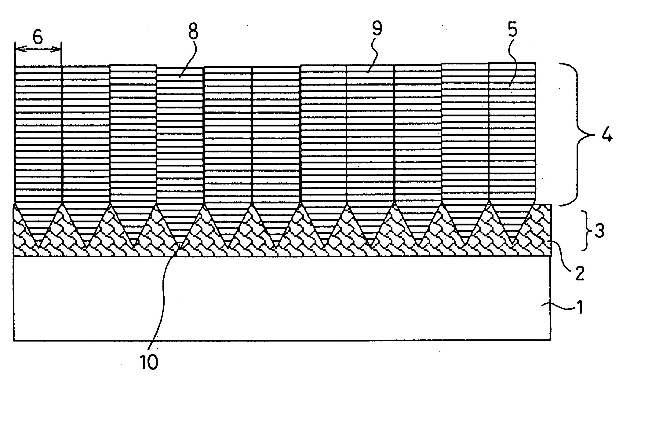
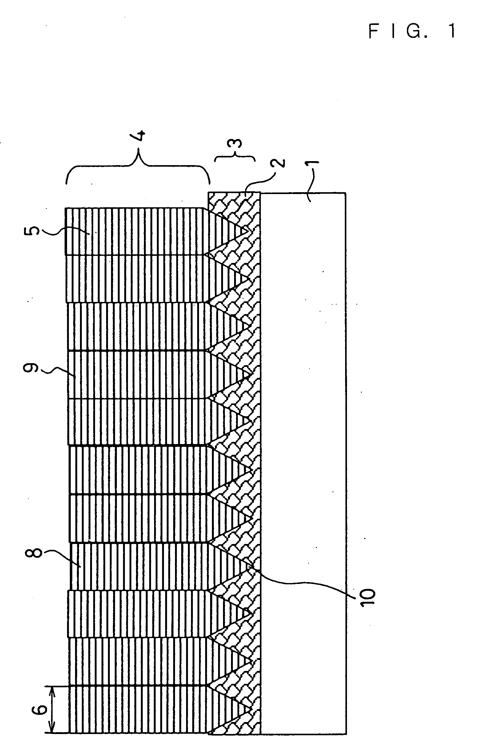
  • Flexible printed circuit board and process for producing the same
  • Flexible printed circuit board and process for producing the same
  • Flexible printed circuit board and process for producing the same

Examples


embodiment 1

[0133] In a film-forming apparatus in accordance with Embodiment 1 of the method for producing the flexible printed circuit board in accordance with the present invention, high-frequency power from a high-frequency oscillator is applied to a conductive substrate holder for holding a plastic film substrate, and glow discharge is generated, whereby the plastic film substrate subsequently becomes the negative electrode of the glow discharge. During this glow discharge, vaporized metal is excited or dissociated or ionized, and vacuum-evaporated on the substrate. The film-forming apparatus for use in Embodiment 1, into which an inert gas, such as argon, or a nitrogen gas is introduced, is used under reduced pressure.

[0134]FIG. 10 is a cross-sectional view showing the schematic configuration of the film-forming apparatus for use in Embodiment 1. In FIG. 10, a tungsten board 25 serving as an evaporation source and a conductive substrate holder 32 serving as a negative electrode are provid...

embodiment 2

[0146] Next, in a film-forming apparatus in accordance with Embodiment 2 of the method for producing the flexible printed circuit board in accordance with the present invention, high-frequency power from a high-frequency oscillator is applied to a conductive substrate holder for holding a plastic film substrate, and glow discharge is generated, whereby the plastic film substrate subsequently becomes the negative electrode of the glow discharge. During this glow discharge, vaporized metal is excited or dissociated or ionized and vacuum-evaporated on the substrate. The film-forming apparatus for use in Embodiment 2, into which an inert gas, such as argon or a nitrogen gas is introduced, is used under reduced pressure. The film-forming apparatus of Embodiment 2 being the same as the film-forming apparatus of the above-mentioned Embodiment 1 was used.

[0147] First, the plastic film substrate is placed inside the film-forming apparatus, and vacuum pumping is carried out until an ultimate...


PUM

PropertyMeasurementUnit
grain sizeaaaaaaaaaa
fluctuation widthaaaaaaaaaa
diameteraaaaaaaaaa

Abstract

The present invention relates to a flexible printed circuit board which has extremely high adhesion performance and on which very fine circuit patterns can be formed by etching, and to a method for producing the same. In the present invention, in the flexible printed circuit board wherein a copper thin film made of copper or an alloy containing primarily copper is directly formed on at least one side of a plastic film substrate, and copper is formed further on the copper thin film by the electrolytic plating method, the above-mentioned copper thin film has a two-layer structure in which a layer including at least a crystalline structure is formed on the surface side thereof, and the X-ray relative intensity ratio between crystal lattice plane indices (200) / (111) in the above-mentioned crystalline structure is 0.1 or less.

Description

TECHNICAL FIELD [0001] The present invention relates to a flexible printed circuit board for use in the electronic circuits of mobile phones, PDAs (personal digital assistants), notebook personal computers, digital still cameras, liquid crystal displays, etc., and to a method for producing the same. BACKGROUND ART [0002] At present, as a flexible copper-clad laminated sheet for use in mobile electronic apparatuses, a material obtained by bonding copper foil to the surface of a polyimide film or a polyester film with adhesive is a mainstream. In these years, mobile electronic apparatuses are made more compact, lightweight and highly functional, whereby flexible circuit boards having very fine circuit patterns and being excellent in high-frequency characteristics are demanded. For example, as the line space of very fine circuit patterns, a shape measuring 25 μm or less, for example, is demanded, and the demand for higher accuracy is also increasing to meet the need for bare chip mount...

Claims


Application Information

Patent Timeline
Patent Type & Authority Applications(United States)
IPC IPC(8): B32B15/08H05K1/09B32B15/20C23C14/20C23C14/32C25D5/10C25D7/06H01B5/14H01B13/00H05K1/00H05K1/03H05K3/00H05K3/38
CPCC25D5/10C25D7/0614H05K1/0393Y10T428/1291Y10S428/901Y10T428/24917H05K3/388C25D5/617H05K1/09C23C14/32H05K3/38
Inventor HIRANAKA, KOUICHINAKAGAMI, RYUICHIFUKUOKA, MITSUHIROYAMASHITA, MOTOHIRO
Owner PANASONIC CORP
Learn More