Silicon-on-insulator active pixel sensors

a silicon-on-insulator and active pixel technology, applied in the field of semiconductor imaging devices, can solve the problems of scaling that can adversely affect the performance of imagers, requires specialized silicon processing that is incompatible with cmos technology, and requires high voltage clocks, so as to reduce the susceptibility to transient effects, reduce the volume of pixels, and increase radiation hardness

Active Publication Date: 2005-09-22
LADARSYST INC
View PDF25 Cites 152 Cited by
  • Summary
  • Abstract
  • Description
  • Claims
  • Application Information

AI Technical Summary

Benefits of technology

[0029] Sensor performance as exposed to ionizing radiation can be configured using conventional radiation hardening processing, implementing radiation mitigation functions including sub-pixel and sub-frame event removal, using up-the-ramp slope sampling, and reducing pixel volume. In an ionizing radiation environment, the benefits of the smaller pixel volume associated with the ability to form thin SOI layers reduces the susceptibility to the transient effects of multiple electron-hole pairs produced by charged cosmic rays, gamma rays, neutrons, and proton events, and increases radiation hardness against non-ionizing displacement damage to the silicon by decreasing the radiation cross-section. While sub-frame and sub-pixel removal of the signal from electron-hole pairs created by transient radiation can be performed in larger pixels, such radiation mitigation comes at the cost of signal amplitude. With small pixels and high frame rate readout, signal losses associated with radiation event removal are limited to a fraction of a pixel or integration time. Small pixels also exhibit lower thermal noise and thus have superior noise performance.
[0030] Atomic displacement caused by impacts of heavy particles (p, n, π, . . . ) results in lattice damage and creates traps in the band-gap. For example, particles with energies of just 25 eV can displace silicon atoms from their lattice points. The resulting crystal lattice contains voids where the silicon atoms have been displaced and clusters where the silicon atoms have come to rest. The significant lattice displacement damage by non-ionizing energy loss (NIEL) mechanisms cause changes that are deleterious for detector lifetime. The most challenging are an increase of the diode volumetric leakage current, due to the introduction of generation centers, and a variation of the full depletion voltage, due to the introduction of deep acceptor defects. A depletion voltage increase r

Problems solved by technology

CCDs, however, are high capacitance devices that require high voltage clocks, consume large amounts of power, provide only serial output, and require specialized silicon processing that is incompatible with CMOS technology.
The expected scaling of MOS devices to even smaller geometries will improve the operation and application of CMOS-based integrated circuits, but such scaling can adversely affect the performance of imagers.
Photoelectrons generated within a depletion region are efficiently collected while photoelectrons generated outside the depletion region are collected only inefficiently, and can diffuse into adjacent pixels.
Therefore, CMOS imagers implemented using an unmodified sub-micron CMOS technology generally exhibit a lower quantum efficiency and increased cross-talk compared to imagers implemented with a lower resolution fabrication process.
Increased cross-talk can lead to degraded color performance and smear.
However, the low NA doping is most often incompatible with conventional CMOS processes.
Another problem in imagers made using bulk-CMOS technology is a rise in photodiode leakage curren

Method used


Image

  • Silicon-on-insulator active pixel sensors
  • Silicon-on-insulator active pixel sensors
  • Silicon-on-insulator active pixel sensors

Examples


Embodiment Construction

[0053] Disclosed below are representative embodiments of methods, apparatus, and systems associated with optical and charged particle sensors. For convenience, these examples are described in a particular sequential order using specific combinations of features. The disclosed methods, apparatus, and systems should not be construed as limiting in any way. Instead, the present disclosure is directed toward all novel and nonobvious features and aspects of the various disclosed embodiments, alone and in various combinations and subcombinations with one another. Further, the disclosed methods, apparatus, and systems are not limited to any specific aspect, feature, or combinations thereof, nor do the disclosed methods, apparatus, or systems require that any one or more specific advantages be present or problems be solved. Method steps are described in a particular order for convenience only, and other orders can generally be used.

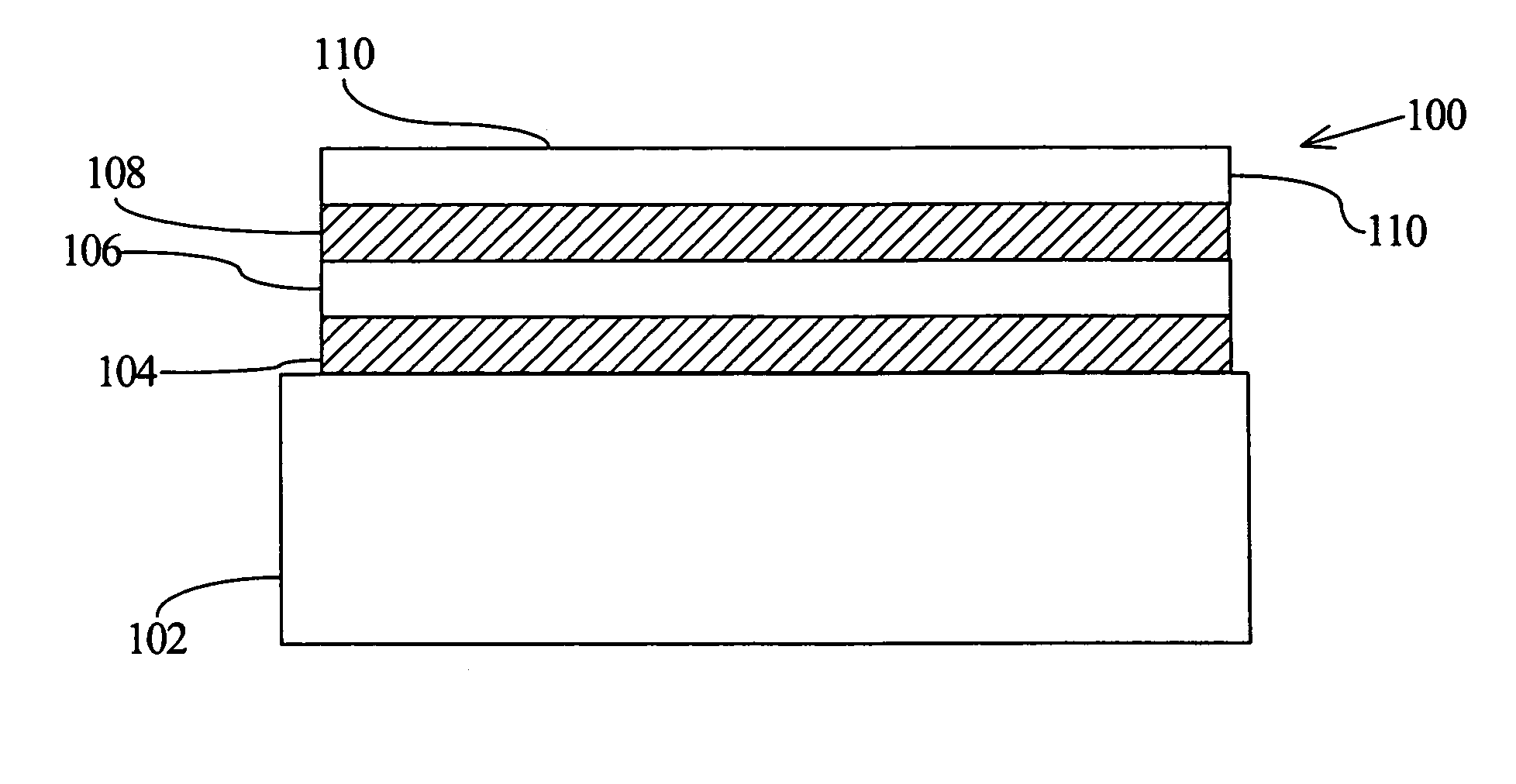
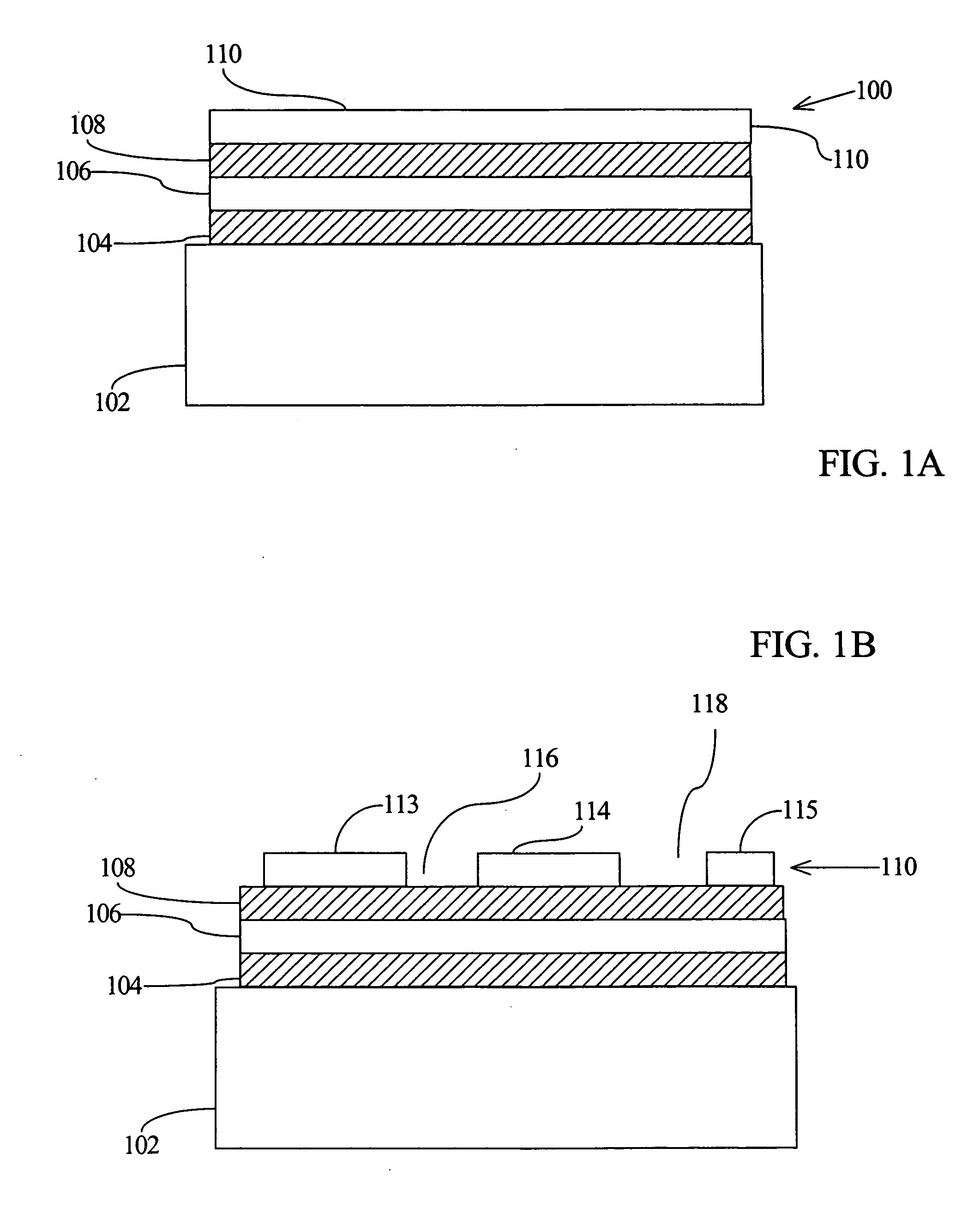
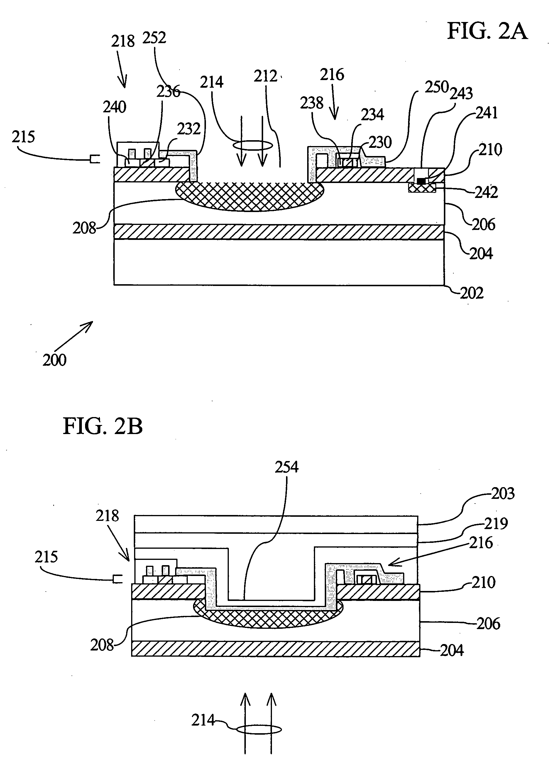
[0054] Sensitive, radiation-tolerant imagers can be fabric...


PUM


Abstract

Active pixel sensors are defined on double silicon on insulator (SOI) substrates such that a first silicon layer is selected to define radiation detection regions, and a second silicon layer is selected to define readout circuitry. The first and second silicon layers are separated by an insulator layer, typically an oxide layer, and the layers can be independently doped. Doping can be provided in the silicon layers of the SOI substrate during assembly of the SOI substrate, or later during device processing. A semiconductor substrate that supports the first and second layers can be removed for, for example, back side radiation detection, using a second insulator layer (typically an oxide layer) as an etch stop.

Description

RELATED APPLICATIONS [0001] This application claims the benefit of U.S. Provisional Application No. 60 / 521,299, filed Mar. 16, 2004 which is incorporated herein by reference.TECHNICAL FIELD [0002] The disclosure pertains to semiconductor imaging devices and methods of manufacturing such devices. BACKGROUND [0003] Image sensors find applications in a wide variety of fields, including machine vision, robotics, astronomy, navigation, as well as consumer products. While complementary metal-oxide-semiconductor (CMOS) technology has provided the foundation for advances in low-cost, low-power, reliable, highly integrated systems for many consumer applications, charge coupled devices (CCDs) have been, until recently, the primary technology used in electronic imaging applications. CCDs, however, are high capacitance devices that require high voltage clocks, consume large amounts of power, provide only serial output, and require specialized silicon processing that is incompatible with CMOS te...

Claims


Application Information

Patent Timeline
IPC IPC(8): H01L21/00H01L21/762H01L21/84H01L27/12H01L27/146
CPCH01L21/76254H01L21/84H01L27/1203H01L27/14609H01L27/1469H01L27/14634H01L27/14643H01L27/14689H01L27/1463
Inventor WILLIAMS, GEORGE MELVILLE JR.
Owner LADARSYST INC
Why Eureka
Try Eureka