
Circuit and method for enhanced low frequency switching noise suppression in multilayer printed circuit boards using a chip capacitor lattice

a multi-layer printed circuit board and chip capacitor technology, applied in the direction of cross-talk/noise/interference reduction, printed capacitor incorporation, printed element electric connection formation, etc., can solve the problems of increasing board thickness, not usually desirable, and increasing cost, so as to improve the suppression of electromagnetic coupling and switching noise

Inactive Publication Date: 2005-10-13
WEMTEC
View PDF5 Cites 45 Cited by
  • Summary
  • Abstract
  • Description
  • Claims
  • Application Information

AI Technical Summary

Benefits of technology

[0011] By way of introduction only, the present embodiments provide a two-dimensional, periodic, metallo-dielectric structure, which acts as a distributed microwave bandstop filter integrated into a parallel-plate waveguide. These embodiments can be used as an electromagnetic interference (EMI) filter to suppress digital noise on power planes, as well as to eliminate power plane resonances. Hence, they may be used for EMI and EMC (electromagnetic compatibility) purposes in printed circuit boards. The periodic structures disclosed herein have electromagnetic stopbands and passbands for TEM-like modes that propagate in parallel-plate waveguides. Therefore, these structures share characteristics of electromagnetic bandgap (EBG) filter concepts. The embodiments described herein extend the lower edge of the fundamental (i.e. lowest frequency) stopband of similar reference structures to well below several hundred MHz.
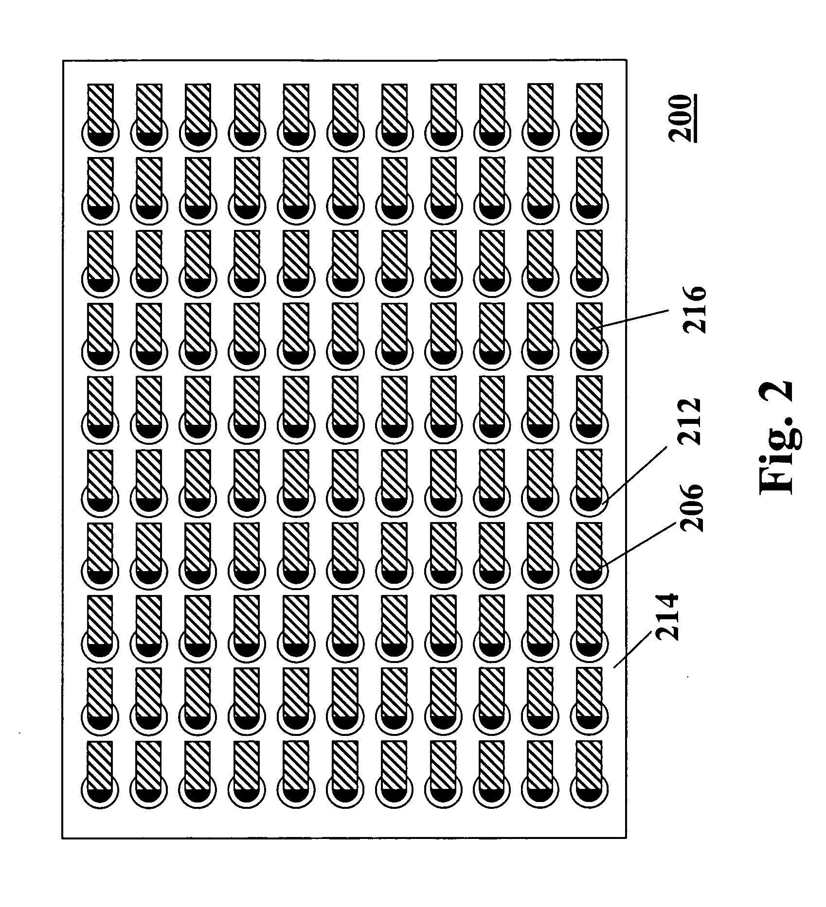
[0013] Although surface mount technology (SMT) capacitors are relatively inexpensive to add to a PCB design, several problems exist with the placement of only a few scattered capacitors around a chip. Isolated capacitors have practical high frequency limits of about 1 GHz or less due to the parasitic series inductance of vias used to connect the bypass capacitor between +Vcc and ground layers. Also, apart from the vias, the parasitic inductance inherent in the capacitors reduces the high frequency limit of operation.
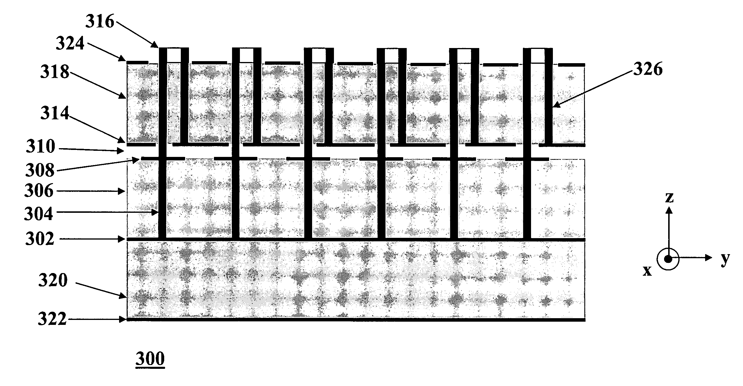
[0014] In particular embodiments, a new structure may be formed as part of a PCB power distribution network to reduce noise coupled from digital switching circuits to power and ground planes of the PCB. With current PCB technology, only a limited amount of capacitance can be realized with parallel plates. For example, a square parallel plate capacitor with sides of 250 mils that are separated by a dielectric material having a thickness of 2 mils and dielectric constant of 4.3 has a capacitance of 30 pF. Use of conventional SMT chip capacitors with much greater values of capacitance (e.g., 500 pF, 1800 pF, or more) that are connected with vias between the buried patches and the upper conducting plane increases the overall capacitance of the structure. The vias connecting the buried patches to the ground plane are actually extended toward the upper plane and are connected to the upper plane through the SMT capacitors. The addition of an SMT capacitor in substantially every cell of the structure enables the lower cutoff frequency of the fundamental stopband to be extended below 50 MHz.
[0017] Adding an array of conventional SMT capacitors to a noise-mitigating structure containing an array of buried patches can extend the low-frequency cutoff from 1 to 2 GHz to 50 MHz or less. Therefore, cutoff may be realized from very low in frequency to 10 GHz using arrays of buried patches with arrays of SMT capacitors.
[0018] Thus, an isolated capacitor is useful for decoupling noise from power planes up to a maximum frequency of 100-500 MHz, depending upon the capacitance of the capacitor. An array of similar SMT capacitors even without buried patches extends the upper frequency cutoff of an isolated capacitor to much higher frequencies, such as 3 to 4 GHz in examples shown here. This example elucidates the power of lattice structures for exhibiting electromagnetic bandgap performance that is not evident from the individual components comprising the lattice. Thus, embodiments comprising arrays of buried patches and SMT capacitors offers significantly improved suppression of electromagnetic coupling and switching noise in power distribution networks over what has been attainable in conventional designs using isolated bypass capacitors alone or structures consisting of buried patches alone.

Problems solved by technology

However, this is not usually desirable since it leads to a smaller stopband bandwidth.
Increasing the via inductance may be accomplished by decreasing the via diameter, which adds cost, or increasing the length of the via, which adds to the board thickness.
Although surface mount technology (SMT) capacitors are relatively inexpensive to add to a PCB design, several problems exist with the placement of only a few scattered capacitors around a chip.
Also, apart from the vias, the parasitic inductance inherent in the capacitors reduces the high frequency limit of operation.
With current PCB technology, only a limited amount of capacitance can be realized with parallel plates.

Method used


Image

  • Circuit and method for enhanced low frequency switching noise suppression in multilayer printed circuit boards using a chip capacitor lattice
  • Circuit and method for enhanced low frequency switching noise suppression in multilayer printed circuit boards using a chip capacitor lattice
  • Circuit and method for enhanced low frequency switching noise suppression in multilayer printed circuit boards using a chip capacitor lattice

Examples


first embodiment

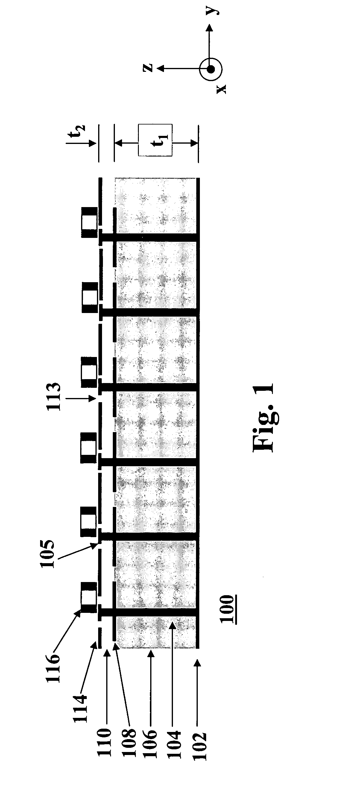
[0046] Referring now to the drawings, FIG. 1 illustrates a parallel plate wave guide (PPW) 100 containing a transverse electromagnetic (TEM) mode suppression circuit. FIG. 1 is a cross-sectional view of the PPW 100. The PPW 100 includes a lower metal layer 102, an upper metal layer 114. Disposed a distance t2 from the upper metal layer is a third metal layer 108 which forms buried patches. Metal layers 108 and 114 are separated by a dielectric layer 110 of thickness t2. Metal layers 102 and 108 are separated by a dielectric layer 106 of thickness t1. An array of conductive rods 104 of length t1+t2 and radius a extend between the lower layer 102 and the upper layer 114. Unless otherwise noted, the dimensions shown in the figures do not include the thickness of the conductive surfaces, which may be a relatively thin metal. The conductive rods may be solid metal poles or may be plated through holes (vias) whose edges are coated with metal but whose centers remain empty. The conductive ...

embodiment 800

[0059] In the embodiment of FIG. 8, SMT capacitors 816 and 828 are located on both sides of the PCB 800 and are connected to the Vcc plane 814 and the ground plane 802 through vias 804 and 826. Again, only one dielectric layer 806 is used to separate the Vcc plane 814 and ground plane 802 since there are no buried patches. The signal layers 822, 824 contain traces that carry digital transmissions between various chips and also make connections to discrete components in addition to the capacitors 828. Dielectric layer 820 separates the ground plane 802 from signal layer 822, while dielectric layer 818 separates the Vcc plane 814 from signal layer 824. This configuration yields more capacitance per unit cell than those having a capacitor on only one side of the board. Alternatively, the embodiment 800 allows greater flexibility in the PCB layout since capacitors may be removed on one side of the board in order to make room for chips while still remaining on the opposite side of the bo...


PUM


Abstract

A printed circuit board (PCB) uses arrays of chip capacitors over the entire surface of the PCB. The PCB includes an upper conductive surface routing signals to components of the PCB, a lower conductive surface, vias between the upper and lower surfaces, and a layer of patches disposed between the upper and lower surfaces to which the vias and chip capacitors are connected. The chip capacitors connect the vias to the upper conductive surface. The use of chip capacitors in a periodic lattice extends the frequency range for suppressing noise in power planes of isolated capacitors from several hundred MHz or less to 4 GHz. Combining the capacitors along with the buried patches extends the low frequency cutoff of high frequency reference noise suppression circuits to 50 MHz or less.

Description

BACKGROUND [0001] This invention is related generally to reduction of noise induced in power planes due to switching of digital circuits in multilayer printed circuit boards. More particularly, the present invention is related to circuits and method for suppression of transverse electromagnetic modes in parallel plate waveguides. [0002] A common problem in electronic systems is switching noise induced in the power distribution system by the operation of digital circuits in the system. Conventionally, such a system has one or more power planes designated, for example, +Vcc, and one or more ground planes. The potential difference between the power plane and the ground plane provides operating voltage for the circuits of the system. If the system includes digital or other circuits with fast-switching outputs, noise can be induced in the power planes and even in the ground plane. The noise may have several sources, but generally is due to the high slew rate of the digital output and the...

Claims


Application Information

Patent Timeline
Patent Type & Authority Applications(United States)
IPC IPC(8): H01L23/50H01L29/00H05K1/02H05K1/11H05K1/16H05K3/42
CPCH01L23/50H01L23/552H01L2924/19105H01L2924/3011H05K1/0216H05K1/0231H05K1/116H05K1/162H05K3/429H05K2201/0191H05K2201/09481H05K2201/09618H05K2201/09672H05K2201/09681H05K2201/09781H01L2924/0002H01L2924/00
Inventor ROGERS, SHAWN D.MCKINZIE, WILLIAM E. III
Owner WEMTEC
Learn More