Dielectric/barrier rib composition for plasma display panel and manufacturing method thereof

a technology of dielectric/barrier rib and plasma display panel, which is applied in the direction of instruments, address electrodes, static indicating devices, etc., can solve the problems of deterioration of dielectric performance, difficult to obtain a low temperature calcination type transparent dielectric material without adding an excess amount of pb, and defective display panels

Active Publication Date: 2005-10-20
KOREA ADVANCED INST OF SCI & TECH
View PDF6 Cites 12 Cited by
  • Summary
  • Abstract
  • Description
  • Claims
  • Application Information

AI Technical Summary

Problems solved by technology

Also, metal Pb remaining inside the film after calcination lowers the breakdown voltage of the dielectric layer, thus resulting in deterioration of dielectric performance.
When utilizing a frit containing a low melting point glass as a main component, it is still difficult to obtain a low temperature calcination type transparent dielectric material without addition of an excess amount of Pb.
Similarly, the low melting point glass paste also requires high temperature calcination at a temperature of 550° C. to 580° C. A thermal hysteresis process at high temperature of more than 500° C. causes many disadvantages such as changes in the dimensions of the glass substrate, patterns that cross each other which results in defective display panels, and difficulty in realizing a large screen of the panel.
The low melting point glass containing primarily Pb has disadvantages such as a high dielectric constant of 10 to 12 and increased power consumption of the device due to generation of high current upon discharging.
In particular, the manufacturing of the barrier rib of the back panel produces a large amount of waste materials, thus increasing environmental contamination and waste material disposal costs.
However, when glass to which a softening point lowering component has been added is used in the dielectric layer, there is a possibility of yellowing in the dielectric layer or front glass panel.
Glass compositions containing a softening point lowering component base limit the use of general substrates such as inexpensive soda lime glass or plastic substrate due to the high calcination temperature of more than 500° C.
Screen-printing is usually used to form the dielectric layer employing the low melting point glass paste, but this process is very complicated due to formation of a thick film by repeated printing more than two times. In particular, the barrier rib of the back panel requires a relatively thick film as compared to the dielectric layer, and requires printing about eight times. However, the film utilizing glass paste shows changes in the flatness of the surface thereof depending on calcination conditions, thus careful attention is required in performing the process.
This transfer method using a dry film simplifies the process, however, defects still occur in the dielectric due to calcination conditions because of the use of the conventional low melting point glass paste.
In addition, high power consumption of the plasma display panel functions as a disadvantage compared to a liquid crystal display (LCD) or organic OLED display device.
High power consumption is due to the high dielectric constant of the dielectric layer (more than 10).
However, in preparing a HDTV grade plasma display panel having a size greater than 60 inches, smaller pitches between the structures and very low surface roughness are required, the screen printing through multi-layer printing or the sandblasting method is not suitable for preparing complex structures having precise dimensions.
Even though this method can simplify the process, it is not possible to avoid disadvantages such as limitation of substrate represented by the calcined low melting point glass, difficulty in patterning a microstructure, surface flatness, and the production of a large amount of environmental contamination waste material.

Method used


Image

  • Dielectric/barrier rib composition for plasma display panel and manufacturing method thereof
  • Dielectric/barrier rib composition for plasma display panel and manufacturing method thereof
  • Dielectric/barrier rib composition for plasma display panel and manufacturing method thereof

Examples


example 1

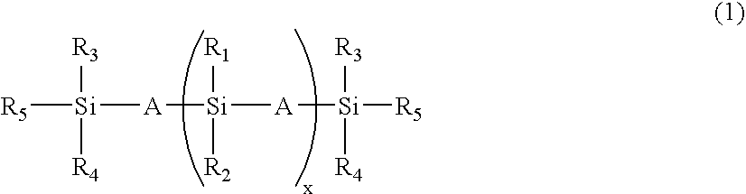
[0042] To PDMS having a vinyl group (molecular weight: 28,000, Bayer) was added 5% by weight of 2,5-dimethyl-2,5-t-butylperoxy hexane (Aldrich) as a cross-linking agent. The mixture was then coated to a thickness of about 30 μm on a glass substrate having ITO vapor deposited thereon using a spin coating or bar coating method, and then cross-linked at a temperature of 150° C. for 1 hour to prepare a dielectric. DC (direct current) breakdown voltage of the dielectric was measured according to ASTM D149. Each electrode had a spherical shape with a diameter of 12.7 mm, and a short period test method was used in which voltage was applied constantly to a test electrode starting at 0 volt and increasing until dielectric breakdown occurred. The dielectric constant was measured with an LCR meter, and transmittance was measured using UV-visible spectroscopy (see Table 1).

example 2

[0043] 10 g of polydimethylsiloxane bis(3-aminopropyl) terminated (molecular weight: 27,000, Aldrich) and 2.2 g of pyromellitic dianhydride were dissolved in 30 g of N-methyl-2-pyrollidone and were subjected to a condensation reaction under nitrogen atmosphere for 12 hours to prepare polyamic acid solution. The resulting solution was coated in the same manner as in Example 1 and cured at temperatures of 100° C., 200° C., and 300° C. for 1 hour, respectively, to obtain a polyimide-siloxane dielectric having a thickness of 20 μm. The subsequent procedure is the same as in Example 1.

example 3

[0044] Divinyl siloxane bis-benzocyclobutene (Dow Chemical) was coated on the ITO coated glass substrate using the same manner as used in Example 1 and then cured at 180° C. for 2 hours to prepare a dielectric film having a thickness of 20 μm. The subsequent procedure is the same as in Example 1.


PUM

PropertyMeasurementUnit
thicknessaaaaaaaaaa
temperatureaaaaaaaaaa
DC breakdown voltageaaaaaaaaaa

Abstract

Provided is a dielectric / barrier rib composition for a plasma display panel, comprising a compound 1 of the formula or at least one compound belonging to a polyhedral oligosilsesquioxane (compound 2) having R6SiO1.5 as a repeating unit, or comprising inorganic / organic hybrid materials having compounds 1 and 2 as a monomer, wherein X is an integer inclusive 0, R1, R2, R3, R4, R5 and R6 are independently a linear, branched or cyclic C1-C12 hydrocarbon group containing one or more alkyl, alkoxy, ketone, acryl, methacryl, allyl, aromatic, halogen, amino, mercapto, ether, ester, sulfone, nitro, hydroxyl, cyclobutene, carbonyl, carboxyl, alkyd, urethane, vinyl, nitrile, hydrogen, or epoxy functional group, and A is oxygen or NH. The inorganic / organic hybrid materials can be a material composed of an extended matrix, containing silicon and oxygen or nitrogen atoms, and having at least one silicon fraction directly bonded to a substituted or unsubstituted hydrocarbon atom.

Description

[0001] This application claims priority to Korean Patent Application No. 10-2004-0023395, filed Apr. 6, 2004, which is incorporated by reference herein in its entirety. BACKGROUND OF THE INVENTION [0002] 1. Field of the Invention [0003] The present invention relates to a dielectric / barrier rib composition for a plasma display panel, and more particularly to a composition used for forming a transparent dielectric layer and a barrier rib on an electrode for a plasma display panel. [0004] 2. Description of the Related Art [0005] A transparent dielectric for a plasma display panel is disposed on a front panel having an ITO (Indium Tin Oxide) and metal electrode patterned thereon and is made by calcining glass paste, including glass powder having a maximum particle size smaller than an average thickness of a film thereof, to form a film having a thickness of 20 μm to 40 μm, in order to secure high transparency. The glass paste is a mixture of PbO—B2O3—SiO2 based glass powder containing a...

Claims


Application Information

Patent Timeline
Patent Type & Authority Applications(United States)
IPC IPC(8): C03C17/30C03C17/42C08K5/24C09D183/04C09D183/14H01J11/12H01J11/22H01J11/24H01J11/26H01J11/34H01J11/36H01J11/38H01J11/40H01J11/42
CPCC03C17/30C09D183/14C09D183/04Y10T428/31612Y10T428/31663B65H75/38B65H2701/34B65H2701/33B65H2403/30
Inventor BAE, BYEONG-SOOLEE, TAE-HOEO, YOUNG-JOOKIM, JUNG-HWAN
Owner KOREA ADVANCED INST OF SCI & TECH
Why Eureka
Try Eureka