Semiconductor device and a method of making the same

a technology of semiconductor devices and buffer sublayers, applied in semiconductor devices, chemical vapor deposition coatings, coatings, etc., can solve the problems of high sapphire cost, added substantively to the manufacturing cost of the semiconductor devices concerned, and difficult and inefficient dicing, etc., to achieve good crystallinity and reduce the strain of the second buffer sublayer

Inactive Publication Date: 2005-12-01
SANKEN ELECTRIC CO LTD
View PDF3 Cites 113 Cited by
  • Summary
  • Abstract
  • Description
  • Claims
  • Application Information

AI Technical Summary

Benefits of technology

[0043] The insulating layer may be made from either one or more of silicon nitride (SiN), silicon oxide (SiO2), aluminum oxide (Al2O3), titanium oxide (Ti2O3), zirconium oxide (ZrO2), and tantalum oxide (Ta2O3). An insulating film of any of these substances will mitigate the strain of the second buffer sublayer and restrict the generation of two-dimensional electron gas.
[0044] The buffer layer may preferably comprise a plurality of first buffer sublayers, a plurality of second buffer sublayers, and at lea

Problems solved by technology

One of the problems encountered with the sapphire substrate is its hardness, which made dicing very difficult and inefficient.
Another problem is the expensiveness of sapphire, which added substantively to the manufacturing costs of the semiconductor devices concerned.
Still another problem with the sapphire substrate is its low heat conductivity, 0.126 W/cm·K.
Incapable of sufficiently liberating the heat developing during operation of the device, the sapphire substrate deteriorated the performance characteristics of the device such as voltage-withstanding capability and gain.
A further problem manifested itself in conjunction with the heterojunction of the prior art HEMT constituted of GaN and AlGaN layers.
The current paths through the buffer layer provide leakage

Method used


Image

  • Semiconductor device and a method of making the same
  • Semiconductor device and a method of making the same
  • Semiconductor device and a method of making the same

Examples


first embodiment

[0064] The invention will now be described in terms of the HEMT using gallium-nitride-based compound semiconductors according to the invention, with reference had to FIGS. 1-3.

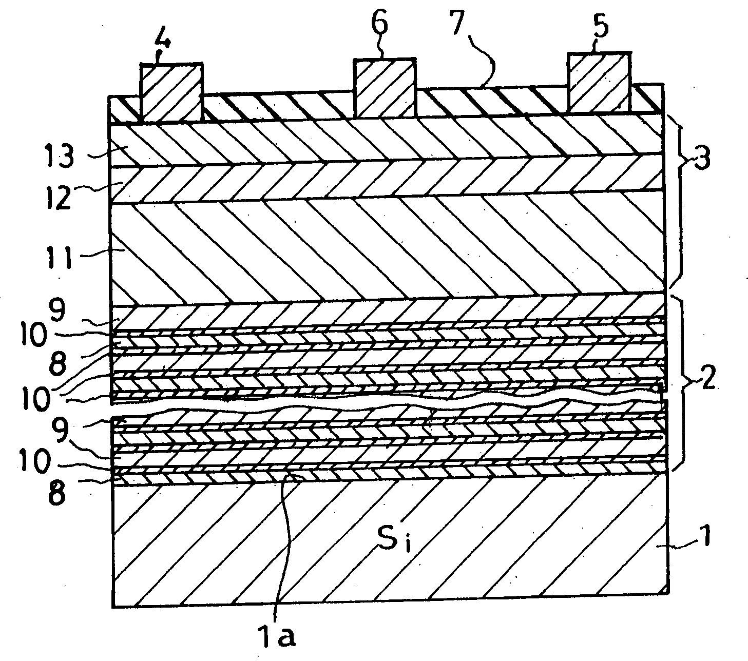
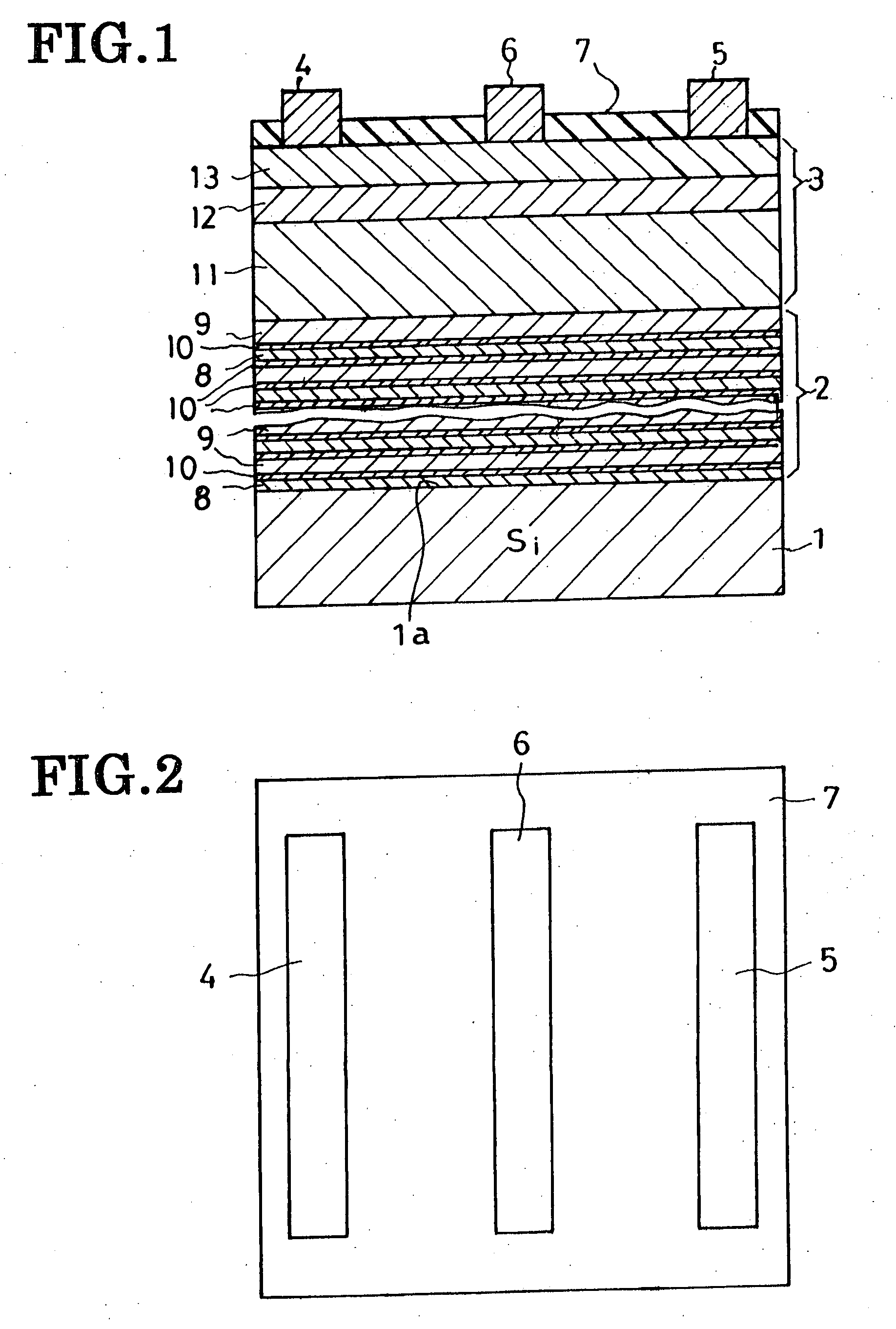
[0065] With reference first to FIG. 1 the HEMT embodying the invention comprises a silicon substrate 1, a buffer layer 2, a main semiconductor region 3 constituting the primary working part of the HEMT, a first electrode or source 4, a second electrode or drain 5, a control electrode or gate 6, and an insulating film 7.

[0066] The substrate 1 is a single crystal of p-type silicon containing boron or other Group III element as a conductivity type determinant. The major surface 1a of the substrate 1, on which there is grown the buffer layer 2, is exactly (111) in terms of Miller indices indicative of crystal face orientation. The impurity concentration of the substrate 1 is set as low as, for example, from 1×1012 cm−3 to 1×1014 cm−3 with a view to the reduction of leakage current through the substrate. The resi...

second embodiment

[0117] Reference may be had to FIG. 4 for a study of a MESFET embodying the principles of this invention. Like reference characters denote like parts in both FIGS. 1 and 4, and the description of such like parts will be omitted.

[0118] The MESFET of FIG. 1 is similar to the HEMT of FIG. 1 except that the main semiconductor region 3 of the latter is modified into an n-type semiconductor region 3a in the form of a layer of a GaN compound semiconductor doped with an n-type impurity of silicon. The MESFET has the silicon substrate 1, buffer layer 2, source 4, drain 5, gate 6 and insulating film 7 which are all equivalent to their FIG. 1 counterparts indicated by the same reference numerals. The n-type semiconductor region 3a, which constitutes the primary working part of the MESFET and which might also be termed a channel layer or active layer, overlies the buffer layer 2. Both source 4 and drain 5 make ohmic contact with the n-type semiconductor region 3a whereas the gate 6 makes Schot...

third embodiment

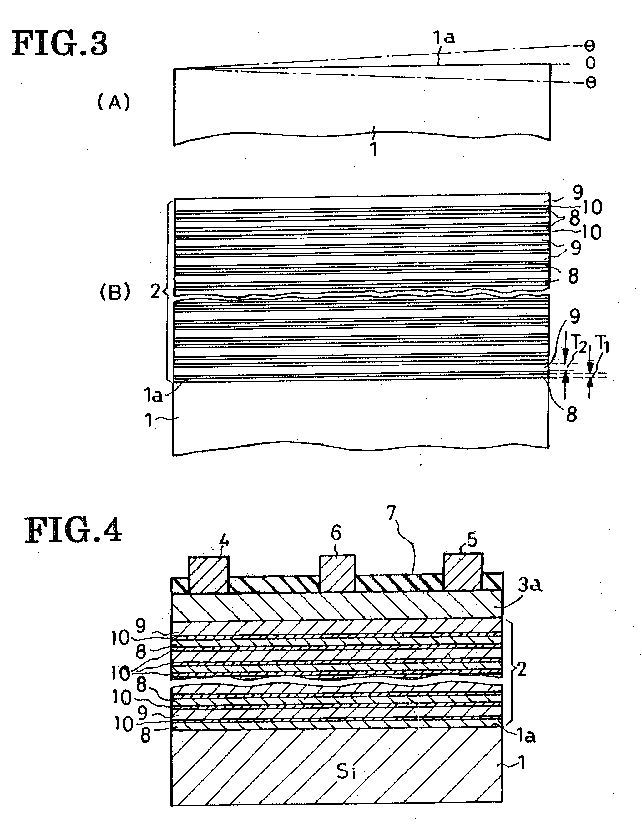
[0121] The buffer layer shown in FIG. 5 and therein generally designated 2a represents a modification of the buffer layer 2 of the two preceding embodiments. The modified buffer layer 2a lends itself to use in both HEMT and MESFET as well as any other semiconductor devices. The modified buffer layer 2a features modified first sublayers 8a, modified second sublayers 9a and unmodified third sublayers 10 of p-type GaN for two-dimensional electron gas. The arrangement of these buffer sublayers 8a, 9a and 10 is the same as that of their counterparts 8-10 in FIGS. 1 and 4.

[0122] The modified first buffer sublayers 8a are made from substances that are generally defined as:

AlxInyGa1-x-yN

where: [0123] 0[0124] 0≦y[0125] x+y≦1.

[0126] No conductivity determinant is added. Examples meeting the above requirements of materials for the modified first buffer sublayers 8a include AlN, AlInN, AlGaN, and AlInGaN. The particular substance employed in this embodiment is Al0.5In0.01Ga0.49N (x=0.5 and...


PUM

PropertyMeasurementUnit
Timeaaaaaaaaaa
Thicknessaaaaaaaaaa
Angleaaaaaaaaaa

Abstract

A semiconductor device having nitride semiconductor layers has a buffer layer (2) in the form of alternations of a first sublayer (8) of AlN and a second layer (9) of GaN with interposition of a third layer (10) of p-type GaN therebetween. On this buffer layer there is grown a main semiconductor region (3) having nitride semiconductor layers for providing a high-electron-mobility transistor or the like. From 0.5 to 50.0 nanometers thick, the third sublayers (10) of the buffer layer restrict the generation of two-dimensional electron gas and so prevent the buffer layer from becoming unnecessarily low in resistance.

Description

CROSS REFERNCE TO RELATED APPLICATIONS [0001] This is a continuation of Application PCT / JP2004 / 000183, filed Jan. 14, 2004, which claims priority to Japanese Patent Application No.2003-010168 filed Jan. 17, 2003. BACKGROUND OF THE INVENTION [0002] This invention relates to semiconductor devices such as metal semiconductor field effect transistors (MESFETs) and high electron mobility transistors (HEMTs) and to a method of fabricating such semiconductor devices. [0003] Semiconductor devices have been known which use gallium-nitride-based compound semiconductors, examples being MESFETs and HEMTs. [0004] In a typical prior art semiconductor device using gallium-nitride-based compound semiconductors, the compound semiconductor region is formed on an electrically insulating substrate of sapphire via a low-temperature buffer layer of GaN or AlN, the latter having been formed with a relatively low substrate temperature of approximately 500° to 600° C. [0005] More specifically, in the case o...

Claims


Application Information

Patent Timeline
IPC IPC(8): C23C16/34H01L21/205H01L21/338H01L29/15H01L29/20H01L29/778H01L29/812
CPCH01L29/155H01L29/7783H01L29/2003
Inventor YANAGIHARA, MASATAKASATO, MASAHIROMOKU, TETSUJI
Owner SANKEN ELECTRIC CO LTD
Why Eureka
Try Eureka