Semiconductor laser device and manufacturing method thereof

a laser device and semiconductor technology, applied in the direction of semiconductor lasers, lasers, solid-state devices, etc., can solve the problems of inability to control the crack of the algan layer, the p-type cladding layer cannot be 0.5 m, and the likely generation of cracks in the algan layer, etc., to achieve low cost, high yield, and low operating current

Active Publication Date: 2005-12-22
PANASONIC CORP
View PDF4 Cites 57 Cited by
  • Summary
  • Abstract
  • Description
  • Claims
  • Application Information

AI Technical Summary

Benefits of technology

[0075] As is clear from the above explanation, according to a semiconductor laser device and the method thereof by the present invention, a semiconductor laser device with high yielding can be realized. In addition, the following semiconductor laser devices can be realized: a low cost semiconductor laser device; a semiconductor laser device of low operating current; a high-output semiconductor laser device; a semiconductor laser device for low threshold current and low operating current; and a long-lived semiconductor laser device.
[0076] In addition, a design margin for following uses can be enlarged: for restraining a generation of a kink in the current-light output characteristics when the high output operation is performed; and for obtaining a stable single horizontal mode high-output laser device. Also, by precisely controlling the difference of the refractive indexes, the design margin in a structural design of a low noise laser device in a self-oscillation type can be enlarged. Further, an interface resistance in a re-grown portion can be smaller and an electrode area on the p-type GaN layer can be bigger. Therefore, a semiconductor laser device of low-operating voltage with small series resistance can be realized. Furthermore, assuming that an n-type AlGaN layer is formed under the n-type GaN cladding layer and the refractive index difference is further set in the cladding layer, it is possible to have a structural design by which light confinement coefficient Tv in a direction perpendicular to the active layer to be held high and a vertical divergence angle θ v to be small. Therefore, a semiconductor laser device with characteristic of high beam usage efficiency in a use of an optical disc for a low threshold current can be realized.

Problems solved by technology

Therefore, it is likely to generate a crack in the AlGaN layer during or after the crystal growth.
Therefore, the methods cannot control the crack of the AlGaN layer.
Therefore, the thickness of the p-type cladding layer cannot be 0.5 μm or thinner so that the methods cannot control the crack of the AlGaN layer.
Further, in the case where the AlGaN is epitaxially grown by the commonly used MOCVD technique, because of a chemical vapor deposition between, for example, an Al source such as Tri-Methyl Aluminum (TMA) and an N source such as NH3, it is difficult to obtain sufficient epitaxial growth-rate.
For example, it is very difficult to obtain a rate of 1 μm / hour and more.
As the result, a growth rate of the epitaxial growth for forming a semiconductor layer including a large amount of AlGaN is decreased so that the conventional laser device in which the AlGaN layer serves as a cladding layer causes high costs due to the long live of the epitaxial growth.

Method used


Image

  • Semiconductor laser device and manufacturing method thereof
  • Semiconductor laser device and manufacturing method thereof
  • Semiconductor laser device and manufacturing method thereof

Examples


first embodiment

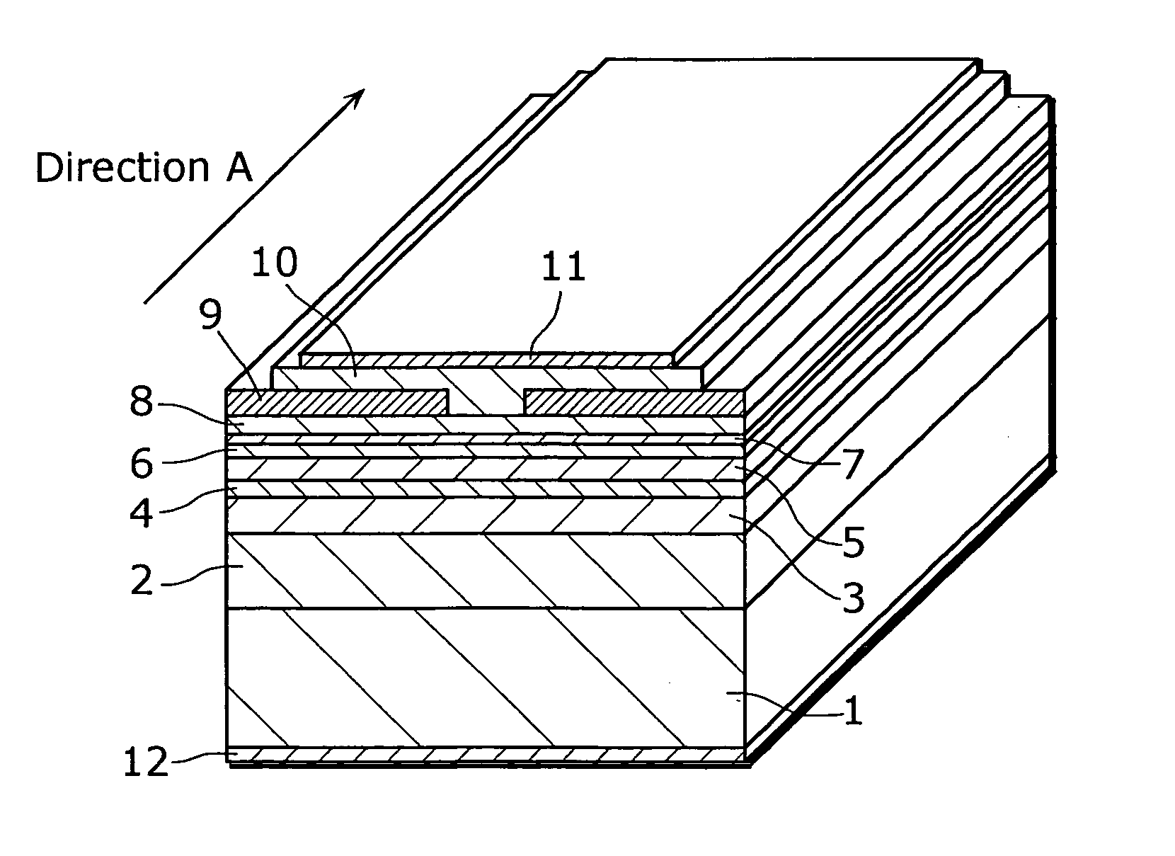
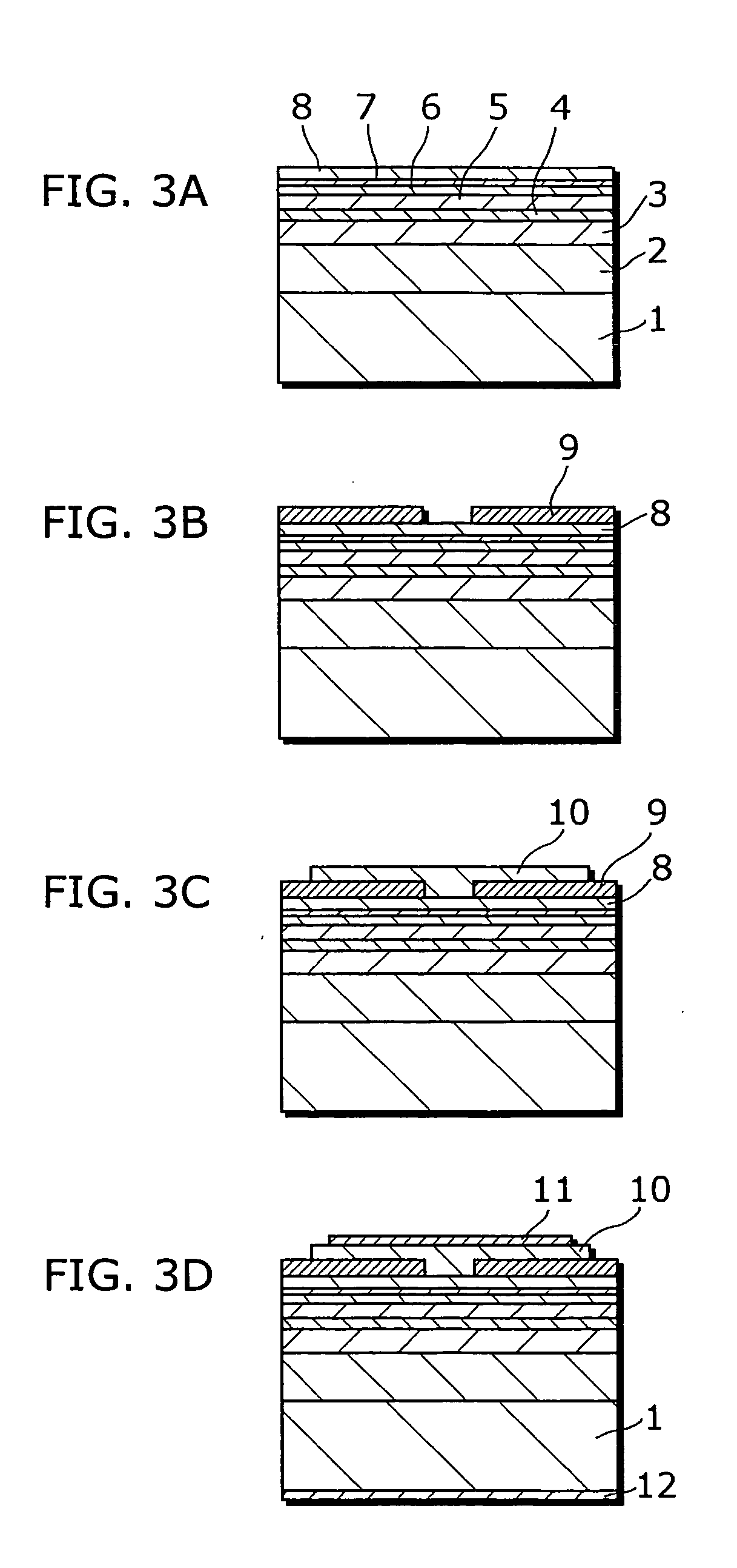
[0101]FIG. 2 is a perspective view showing a structure of a blue-violet semiconductor laser device in a first embodiment.

[0102] The semiconductor laser device has a GaN substrate 1, an n-type GaN layer 2, an n-type AlGaN cladding layer 3, an n-type GaN guide layer 4, an InGaN multiple quantum well active layer 5 as a light-emitting layer, an undoped-GaN guide layer 6, a p-type AlGaN electron overflow suppression layer 7, a p-type GaN guide layer 8 as a light guide layer, an SiO2 blocking layer 9 as a current confinement layer, an Ni / ITO cladding layer electrode 10 as a transparent electrode, a Ti / Au pad electrode 11 and a Ti / Al / Ni / Au electrode 12.

[0103] The following layers are sequentially formed on the GaN substrate 1 by an epitaxial growth technique using, for example, a MOCVD technique and the like: the n-type GaN layer 2; the n-type AlGaN clad cladding layer 3; the n-type GaN guide layer 4; the InGaN multiple quantum well active layer 5; the undoped-GaN guide layer 6; the p-t...

second embodiment

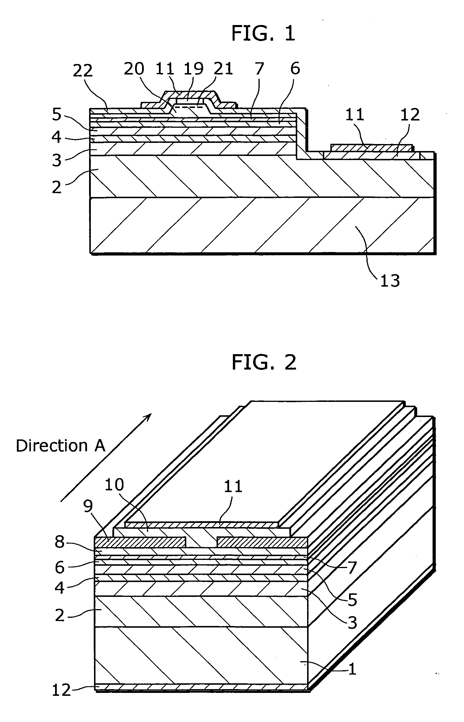
[0120]FIG. 4 is a perspective view showing a structure of a blue-violet semiconductor laser device according to the second embodiment.

[0121] The semiconductor laser device has a sapphire substrate 13, an n-type GaN layer 2, an SiO2 mask 14, an n-type AlGaN cladding layer 3, an n-type GaN guide layer 4, an InGaN multiple quantum well active layer 5, an undoped-GaN guide layer 6, a p-type AlGaN electron overflow suppression layer 7, a p-type GaN guide layer 8, an SiO2 blocking layer 9, an Ni / ITO thin film electrode 16 as a transparent electrode, an Nb2O5 cladding layer 15 as a dielectric layer, a Ti / Au pad electrode 11 and a Ti / Al / Ni / Au electrode 12.

[0122] The following layers are sequentially formed on the sapphire substrate 13 by the epitaxial growth technique using, for example, the MOCVD technique and the like: the n-type GaN layer 2; the n-type AlGaN cladding layer 3; the n-type GaN guide layer 4; the InGaN multiple quantum well active layer 5; the undped-GaN guide layer 6; the...

third embodiment

[0144]FIG. 6 is a perspective view showing a structure of a blue-violet semiconductor laser device according to the third embodiment.

[0145] The semiconductor laser device has an n-type GaN layer 2, an n-type AlGaN cladding layer 3, an n-type GaN guide layer 4, an InGaN multiple quantum well active layer 5, an undoped-GaN guide layer 6, a p-type AlGaN electron overflow suppression layer 7, a p-type GaN guide layer 8, an SiO2 blocking layer 9, an Ni / ITO cladding layer electrode 10, a Ti / Au electrode 30 as a metal film, a Ti / Al / Ni / Au electrode 12, an Au / AuSn / Au / Ni electrode 17 as a metal film, a low resistance SiC substrate 18 and an Ni / Au electrode 19.

[0146] The following layers are sequentially formed on the n-type GaN layer 2: the n-type AlGaN cladding layer 3; the n-type GaN guide layer 4; an InGaN multiple quantum well active layer 5; an undoped-GaN guide layer 6; the p-type AlGaN electron overflow suppression layer 7; and the p-type GaN guide layer 8. Herein, blue-violet light ...


PUM


Abstract

It is an object of the present invention to provide a semiconductor laser device with high-yielding in which a clack generated in an epitaxial growth layer is restrained and to the manufacturing method thereof, the semiconductor laser device includes a GaN substrate 1, an n-type GaN layer 2, an n-type AlGaN cladding layer 3, a n-type GaN guide layer 4, an InGaN multiple quantum well active layer 5, an undoped-GaN guide layer 6, a p-type AlGaN electron overflow suppression layer 7, a p-type GaN guide layer 8, a SiO2 blocking layer 9, an Ni/ITO cladding layer electrode 10 as a transparent electrode, a Ti/Au pad electrode 11, and a Ti/Al/Ni/Au electrode 12. The SiO2 blocking layer 9 is formed above the InGaN multiple quantum well active layer 5 so as to have an opening. The Ni/ITO cladding layer electrode 10 is formed inside the opening, and which is transparent for the light from the InGaN multiple quantum well active layer, and serves as a cladding layer.

Description

BACKGROUND OF THE INVENTION [0001] (1) Field of the Invention [0002] The present invention relates to a semiconductor laser device applicable to a blue-violet semiconductor laser device used for, for example, a light source for writing and reading of a high density optical disc, and a manufacturing method thereof. [0003] (2) Description of the Related Art [0004] A III-V group nitride semiconductor (hereafter referred to as InGaAlN) represented by GaN has been focused as a material which has a large band gap (3.4 eV for GaN in room temperature) and can realize a device which emits light in a wave range from green to ultraviolet light. By now, a green / blue light-emitting diode using the InGaAlN has been commercially manufactured and available for various displays, traffic signals and the like. Also, a white light-emitting diode which emits white light by exciting a phosphor using a blue light-emitting diode and an ultraviolet light-emitting diode has been commercially manufactured and...

Claims


Application Information

Patent Timeline
Patent Type & Authority Applications(United States)
IPC IPC(8): H01L29/06H01S5/042H01S5/20H01S5/223H01S5/343
CPCB82Y20/00H01S5/0208H01S5/0425H01S5/2009H01S5/2214Y10S438/973H01S5/3214H01S5/34333H01S2304/12Y10S438/977H01S5/2231H01S5/04253H01S5/04257
Inventor UEDA, TETSUZOYURI, MASAAKI
Owner PANASONIC CORP
Why Eureka
Try Eureka