Dielectric barrier layer films

a technology of dielectric barrier layer and film, applied in the direction of discharge tube luminescnet screen, discharge tube/lamp details, vacuum evaporation coating, etc., can solve the problems of low coating rate, inability to describe a film that would operate as a good barrier layer for optical devices, and large defect structure of fcva layer for formation of effective optical barrier layers. , to achieve the effect of superior performan

Inactive Publication Date: 2006-04-06
DEMARAY
View PDF69 Cites 75 Cited by
  • Summary
  • Abstract
  • Description
  • Claims
  • Application Information

AI Technical Summary

Benefits of technology

[0015] In accordance with the present invention, one or more dielectric layers formed from layers of metal-oxide materials deposited by a pulsed, biased, wide area physical vapor deposition process are presented. A dielectric barrier layer according to the present invention can be formed from at least one highly densified metal oxide layer. Dielectric barriers according to the present invention can be highly densified, highly uniform, ultra smooth amorphous layers with ultra low concentrations of defects, providing for superior performance as protective layers against physical wear and atmospheric contamination of underlying structures as well as overlying structures that may be deposited to form an electrical, optical, or medical device. Barrier layers according to the present invention can also be self-protecting optical layers, electrical layers, or tribological layers that can be utilized actively in optical or electrical devices.
[0018] In some embodiments, a soft metal (e.g., indium) breath treatment can be utilized before deposition of a barrier layer. Such a breath treatment is shown to significantly improve surface roughness and enhance WVTR characteristics for embodiments of barrier layers according to the present invention.

Problems solved by technology

Morton, et al., therefore fail to describe a film that would operate as a good barrier layer for optical devices.
Lower ion energies are not reported due to the problem of extracting and directing a lower energy ion flux with a useful space charge density.
Due to the limitation of the coating species to the ion flux, coating rates are low.
The defect structures exhibited in the FCVA layer are too large for formation of effective optical barrier layers.
Additionally, ion sputtering of crystalline films is dependent on the crystal orientation, leading to higher surface roughness.
Defect structures formed in a protective layer can degrade the optical quality of the layer and also provide paths for diffusion of atmospheric contaminations through the layer, compromising the protective properties of the layer.
It may be that the high resputtering rate at the high voltages used in this process cause surface roughening.
However, as noted, at ion energies exceeding the chemical threshold, and particularly at energies-exceeding 20 Volts or so, damage to the film or the substrate resulting from the ion energy in excess of the chemical binding energy is significant, and results in surface roughness, increased optical absorption characteristics, and creation of defects.
Charging of the deposited film is also a particular problem with ion beam deposited dielectrics.
To date, no low temperature dielectric and also no ion beam dielectric is known that has ever been shown to provide the electrical quality required for a transistor gate layer, for example.
Consequently, no as-deposited low temperature dielectric, biased or unbiased, has been proposed for low temperature transistor applications or is known at this time.

Method used


Image

  • Dielectric barrier layer films
  • Dielectric barrier layer films
  • Dielectric barrier layer films

Examples


Embodiment Construction

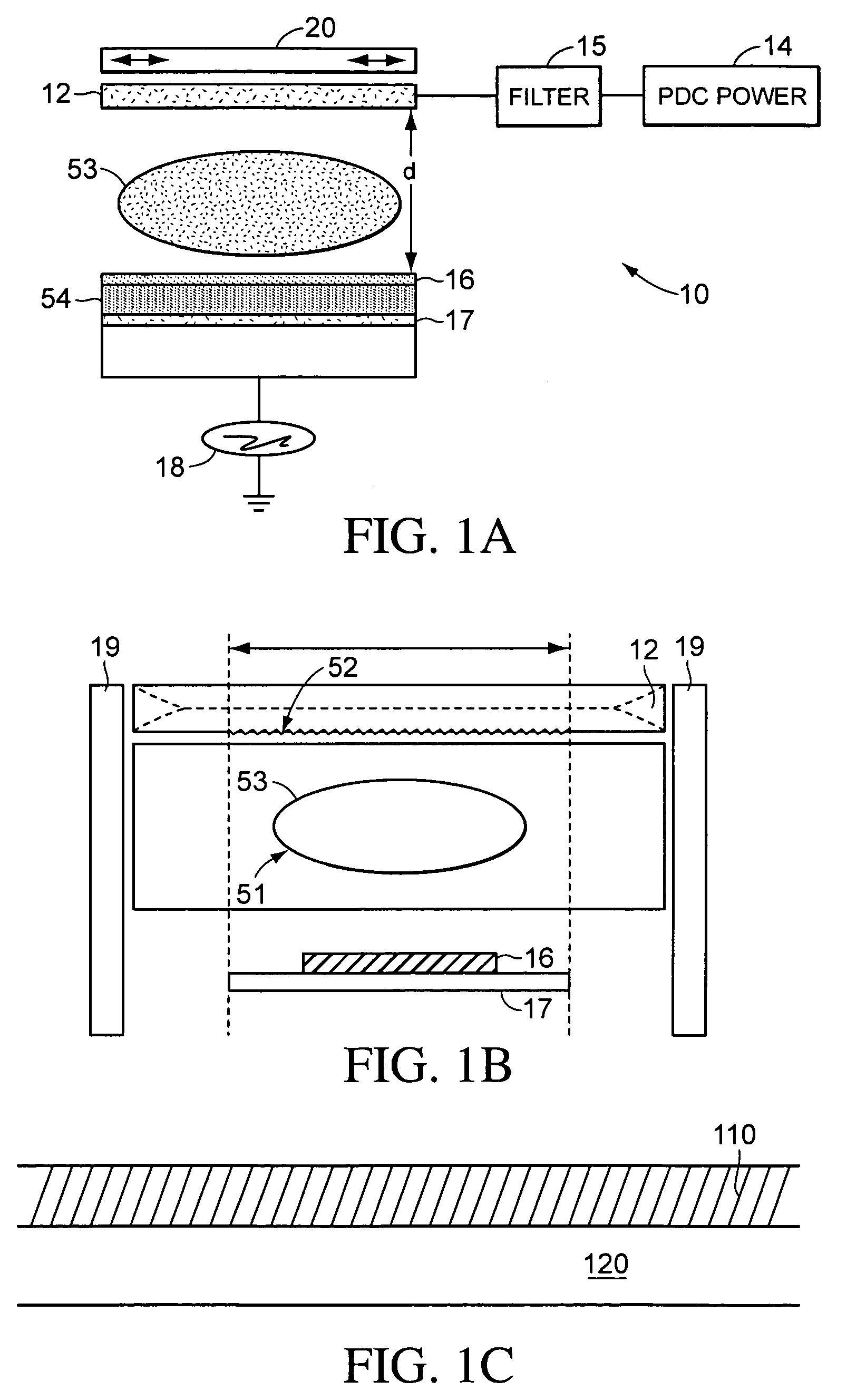
[0044] Barrier layers according to some embodiments of the present invention are deposited in a pulsed-dc, substrate biased, wide target physical vapor deposition process that is described further below with respect to some particular examples of such barrier layers. Some embodiments of barrier layers according to embodiments of the present invention can be characterized as highly densified, highly uniform, highly amorphous layers with particularly low defect concentrations-and high surface smoothness. Further, barrier layers according to embodiments of the present invention can have beneficial optical and electrical characteristics that allow such barrier layers to be self-protecting optical or electrical layers in optical or electrical devices formed with these layers.

[0045] For example, some embodiments of barrier layers according to the present invention can have excellent optical transparency characteristics. Further, the index of refraction of individual barrier layers is dep...


PUM

PropertyMeasurementUnit
humidityaaaaaaaaaa
humidityaaaaaaaaaa
bias voltageaaaaaaaaaa

Abstract

In accordance with the present invention, a dielectric barrier layer is presented. A barrier layer according to the present invention includes a densified amorphous dielectric layer deposited on a substrate by pulsed-DC, substrate biased physical vapor deposition, wherein the densified amorphous dielectric layer is a barrier layer. A method of forming a barrier layer according to the present inventions includes providing a substrate and depositing a highly densified, amorphous, dielectric material over the substrate in a pulsed-dc, biased, wide target physical vapor deposition process. Further, the process can include performing a soft-metal breath treatment on the substrate. Such barrier layers can be utilized as electrical layers, optical layers, immunological layers, or tribological layers.

Description

RELATED APPLICATIONS [0001] The present application claims priority to U.S. Provisional Application 60 / 451,178, “Dielectric Barrier Film,” filed on Feb. 27, 2003, by Richard E. Demaray, Mukundan Narasimhan, and Hongmei Zhang, herein incorporated by reference in its entirety, and to U.S. Provisional Application 60 / 506,128, “Indium Nucleation Layer,” filed on Sep. 25, 2003, by Mukundan Narasimhan and Peter Brooks, herein incorporated by reference in its entirety.BACKGROUND [0002] 1. Field of the Invention [0003] The present invention is related to dielectric barrier films and, in particular, dielectric barrier films formed from high-density optical material layers for utilization in optical, electrical, tribological, and bio-implantable devices. [0004] 2. Discussion of Related Art [0005] Dielectric barrier layers are becoming increasingly important as protective layers for organic light emitting diodes (OLEDs) and other optical or opto-electronic devices. Typically, dielectric barrier...

Claims


Application Information

Patent Timeline
Patent Type & Authority Applications(United States)
IPC IPC(8): H01J1/62C23C14/34C23C14/35H01L21/314H01L21/316H01L51/52
CPCC23C14/345C23C14/35H01L21/02145H01L21/02164H01L21/02178H01L21/02186H01L21/02192H01L21/02194H01L21/022H01L21/02266H01L21/02304H01L21/31604H01L21/31608H01L21/31612H01L21/31616H01L21/31637H01L21/31691H01L51/5237H01L51/5265Y10S438/958H10K50/844H10K50/8445H10K50/852C23C14/34C23C14/02H05B33/22C09K5/00
Inventor NARASIMHAN, MUKUNDANBROOKS, PETERDEMARAY, RICHARD E.
Owner DEMARAY
Why Eureka
Try Eureka