
Dielectric ceramics, multilayer ceramic capacitor and method for manufacturing the same

Active Publication Date: 2006-04-27
KYOCERA CORP
View PDF11 Cites 22 Cited by
  • Summary
  • Abstract
  • Description
  • Claims
  • Application Information

AI Technical Summary

Benefits of technology

[0012] The main advantage of the present invention is to obtain a dielectric ceramics that is composed of crystal grains having a high relative dielectric constant while being atomized.
[0013] The other advantage of the present invention is to obtain a multilayer ceramic capacitor that has high relative dielectric constant, stable temperature characteristic and insulation as well as high reliability, even if dielectric layers have smaller thickness.
[0014] The dielectric ceramics of the present invention has a mean grain size of not more than 0.2 μm, preferably not more than 0.15 μm, and contains crystal grains mainly composed of barium titanate. The crystal grains have a volume per unit cell V of not more than 0.0643 nm3. V is represented by a product of lattice constant (a, b, c) figured out from the X-ray diffraction pattern of the crystal grains. Thereby, the dielectric ceramics of the present invention can attain a high relative dielectric constant.
[0015] The method for manufacturing such a dielectric ceramics comprises the steps of: (a) obtaining dielectric primary powder whose mean grain size is not more than 0.1 μm through any one liquid phase method selected from oxalic acid method, sol-gel method and hydrothermal synthesis method; (b) obtaining dielectric powder by drying and heating the dielectric primary powder with a zeolitic drying agent in the atmosphere of a temperature 300 to 500° C. at atmospheric pressure; and (c) firing a forming body that is molded into a predetermined shape with the dielectric powder.
[0016] The first multilayer ceramic capacitor of the present invention comprises dielectric layers composed of the above-mentioned dielectric ceramics and internal electrode layers. The dielectric layers and the internal electrode layers are alternately laminated.
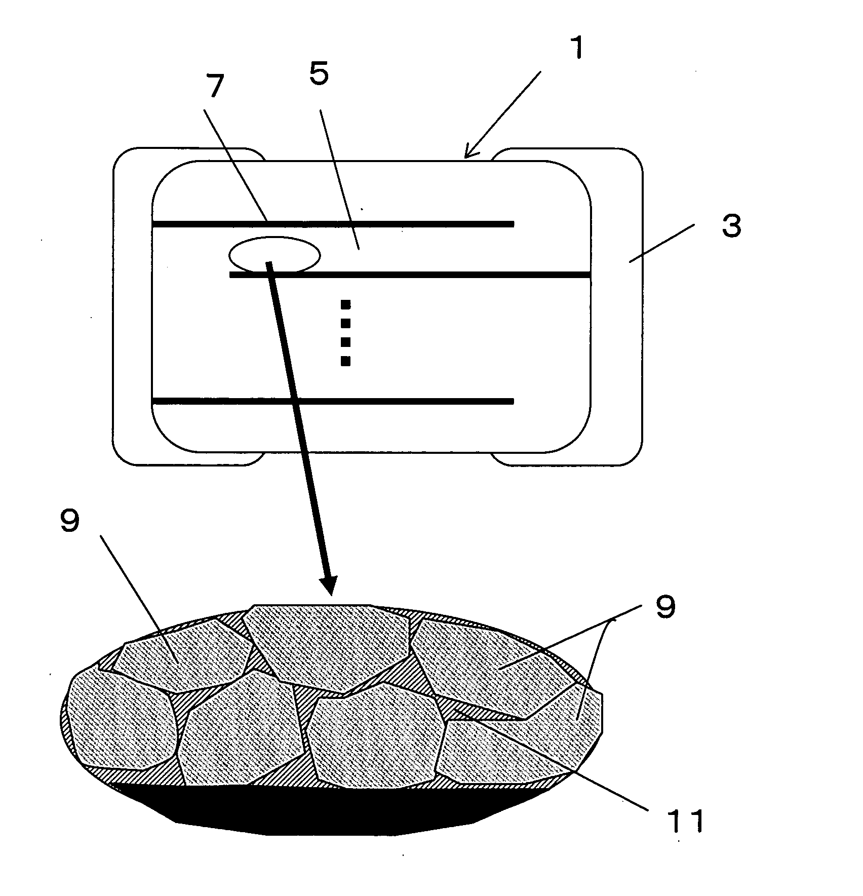
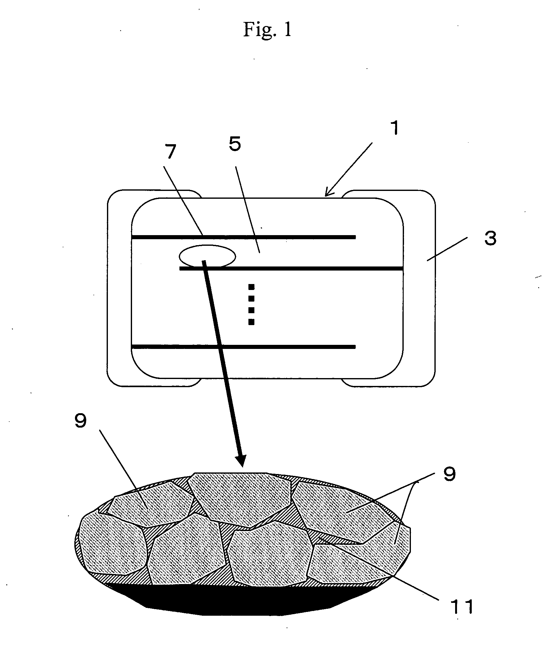
[0017] The second multilayer ceramic capacitor of the present invention comprises a capacitor body wherein dielectric layers and internal electrode layers are alternately laminated. The dielectric layers have crystal grains sintered through a grain boundary layer. (a) Crystal grains constituting the dielectric layer have a mean grain size of not more than 0.2 μm. (b) The crystal grains are mainly composed of barium titanate. (c) When the volume per unit cell Vbulk is represented by a product of lattice constant (a, b, c) figured out from the X-ray diffraction pattern of the dielectric layer, and the volume per unit cell Vpowder is represented by a product of lattice constant (a, b, c) figured out from the X-ray diffraction pattern of crystal grains obtained by grinding the dielectric layer, Vbulk and Vpowder satisfy the relation Of Vbulk / Vpowder≧1.005.

Problems solved by technology

Therefore, there has been a problem that a dielectric ceramics prepared by using the dielectric powder so obtained has a low relative dielectric constant.
However, if fine barium titanate powder according to Japanese Unexamined Patent Publication No. 2003-309036, for example, is used to make dielectric layers thinner in manufacturing a multilayer ceramic capacitor, abnormal grain growth occurs during firing at atmospheric pressure.
Therefore, crystal grains constituting a dielectric layer cannot have uniform grain size, and large crystal grains resulting from grain growth are present in part.
There has been a problem that a multilayer ceramic capacitor having such crystal grains has larger temperature characteristic of relative dielectric constant and lower insulation, in particular, lower reliability in high temperature load test.

Method used


Image

  • Dielectric ceramics, multilayer ceramic capacitor and method for manufacturing the same
  • Dielectric ceramics, multilayer ceramic capacitor and method for manufacturing the same
  • Dielectric ceramics, multilayer ceramic capacitor and method for manufacturing the same

Examples


examples

[0081] The following examples illustrate the manner in which the present invention can be practiced. It is understood, however, that the examples are for the purpose of illustration and the invention is not to be regarded as limited to any of the specific materials or condition therein.

example i

[0082] Regarding the dielectric ceramics of the present invention, the effect of volume per unit cell represented by a product of lattice constant (a, b, c) figured out from X-ray diffraction pattern was checked. First, dielectric primary powders obtained through sol-gel method, hydrothermal synthesis method, oxalic acid method and solid phase method shown in Table 1 were prepared. These powders were prepared so as to have the ratio Ba / Ti of 1.005.

[0083] The next step was to dry powders. When a zeolitic drying agent was not employed, the above powders went through preliminary drying at atmospheric pressure and in the atmosphere of temperature 200° C.

[0084] Meanwhile when a zeolitic drying agent was employed, the dielectric primary powders so prepared went through dry-heat process at atmospheric pressure and 400° C. The zeolitic drying agent used was mainly composed of aluminosilicate and had the specific surface of 600 m2 / g. Thereby, dielectric powders were obtained. The quantity ...

example 2

[0091] First, to check the effect of glass softening point and thermal expansion coefficient, dielectric powder was molded into a 1 mm-thick tablet-like shape having a diameter of 12 mm and fired. Then, evaluation was made. The results were presented as dielectric ceramics in Tables 2 and 3. The mean grain size of barium titanate that was used, the ratio A / B, the ratio c / a, the added amount, firing temperature and glass composition were shown in Tables 2 and 3. By plating, 0.1 parts by weight of Mg, 1 part by weight of Y and 0.2 parts by weight of Mn in terms of oxide to 100 parts by weight of barium titanate powder were contained in the barium titanate powder used here. 1 part by weight of glass component to 100 parts by weight of barium titanate powder was contained in glass powder. The ratio of A site / B site in BT powder used here was 1.003 or 1.001.

[0092] The softening point of glass powder was measured with a TG-DTA after molding glass powder into a tablet-like shape. The ther...


PUM

PropertyMeasurementUnit
Grain sizeaaaaaaaaaa

Abstract

Crystal grains mainly composed of barium titanate have a mean grain size of not more than 0.2 μm. The volume per unit cell V that is represented by a product of lattice constant (a, b, c) figured out from the X-ray diffraction pattern of the crystal grains is not more than 0.0643 nm3. Thereby, a dielectric ceramics having high relative dielectric constant can be obtained. A multilayer ceramic capacitor comprises a capacitor body and an external electrode that is formed at both ends of the capacitor body. The capacitor body comprises dielectric layers composed of the dielectric ceramics, and internal electrode layers. The dielectric layers and the internal electrode layers are alternately laminated.

Description

[0001] Priority is claimed to Japanese Patent Application No. 2004-312454 filed on Oct. 27, 2004, and Japanese Patent Application No. 2004-340347 filed on Nov. 26, 2004, the disclosure of which is incorporated by reference in its entirety. BACKGROUND OF THE INVENTION [0002] 1. Field of the Invention [0003] The present invention relates to a dielectric ceramics, a multilayer ceramic capacitor using the same and a method for manufacturing them. [0004] 2. Description of Related Art [0005] In recent years, as mobile devices such as cellular phones are more widely used and semiconductor devices that are the main part of a personal computer have higher speed and higher frequency, a multilayer ceramic capacitor for these electronics is increasingly required to have small size and large capacity. [0006] To meet such requirement, in a multilayer ceramic capacitor (MLC), efforts have been made for smaller size and larger capacity, by making dielectric layers thinner to enhance electrostatic c...

Claims


Application Information

Patent Timeline
IPC IPC(8): H01G4/06
CPCC04B35/4682C04B35/624C04B35/62655C04B35/62805C04B35/6281C04B35/62815C04B35/645C04B2235/3206C04B2235/3225C04B2235/3262C04B2235/36C04B2235/449C04B2235/5445C04B2235/6025C04B2235/656C04B2235/6562C04B2235/6565C04B2235/6567C04B2235/6582C04B2235/663C04B2235/761C04B2235/762C04B2235/786C04B2235/79C04B2235/85H01G4/1227H01G4/1281H01G4/30
Inventor YAMAZAKI, YOUICHIITOH, YUMIKOKAMIGAKI, KOUSEIMATSUBARA, KIYOSHI
Owner KYOCERA CORP
Learn More