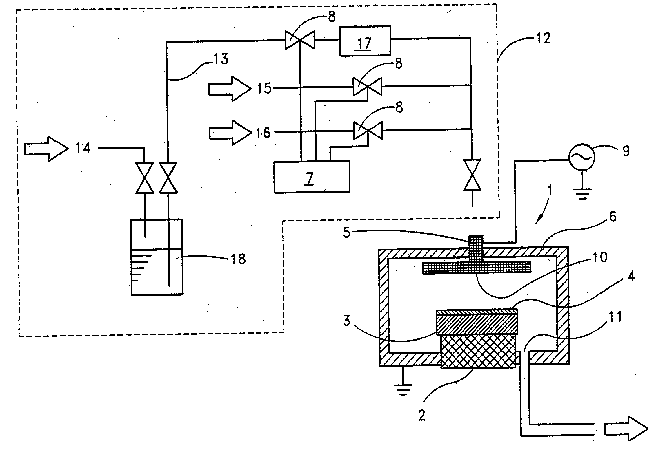
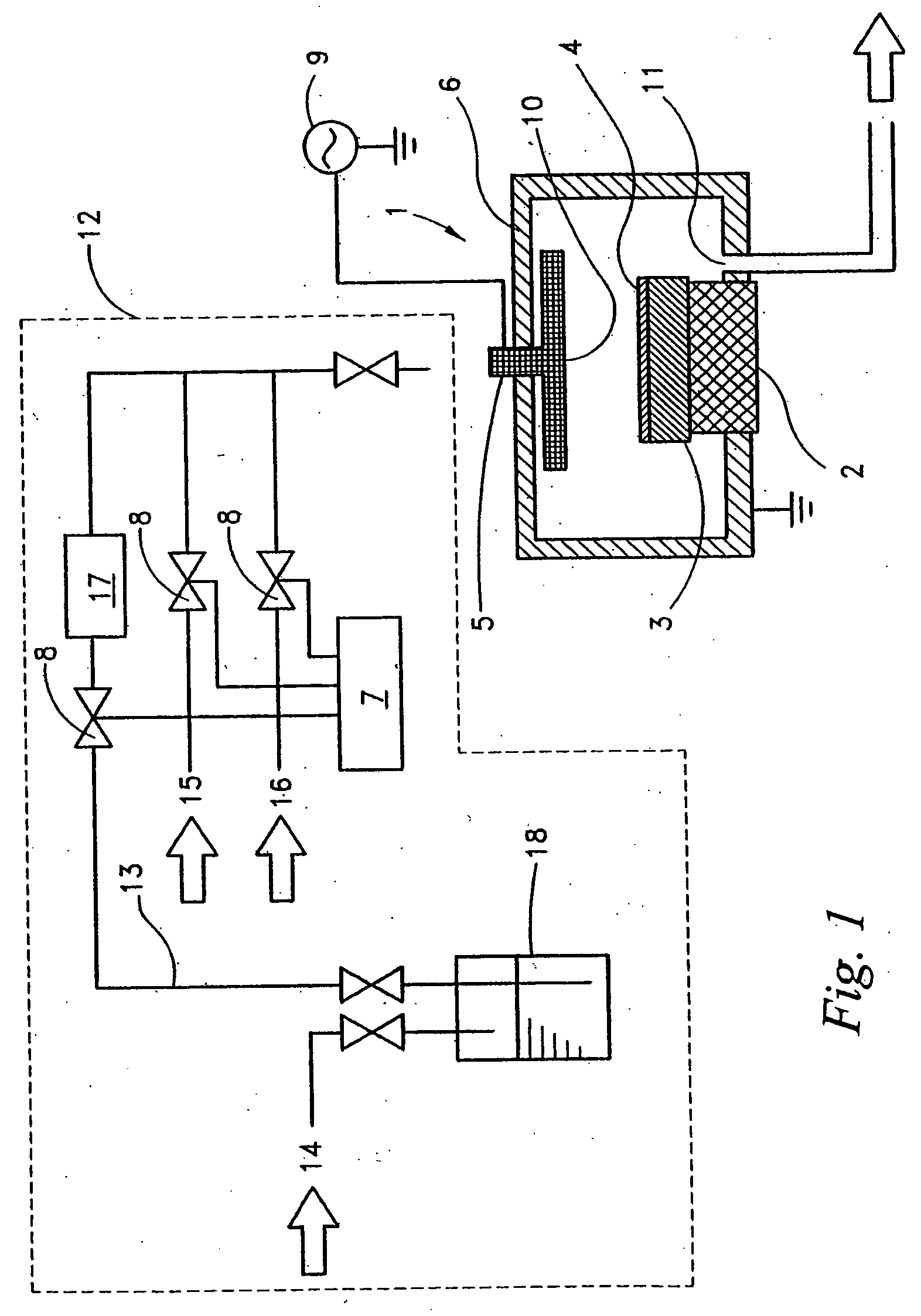
Method for forming insulation film
a technology of insulation film and film density, which is applied in the direction of coating, solid-state device, chemical vapor deposition coating, etc., can solve the problems of affecting high-speed operations, poor adhesion with silicon-containing materials, and low thermal stability of fluorinated amorphous carbon film, so as to reduce the distance between the electrodes, effectively block moisture penetration, and film density can increase
- Summary
- Abstract
- Description
- Claims
- Application Information
AI Technical Summary
Benefits of technology
Problems solved by technology
Method used
Image

Examples
example 1
[0106] The conditions for forming a hard film are as follows:
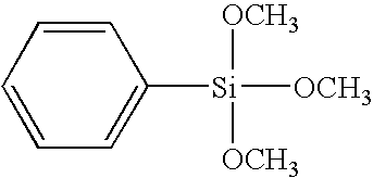
[0107] DMOTMDS (1,3-dimethoxytetramethyl disiloxane): 100 sccm
[0108] He: 100 sccm
[0109] Pr (reaction chamber pressure): 566 Pa
[0110] RF power supply (HF: 27.12 MHz): 400 W
[0111] RF power supply (LF: 400kHz): 100 W
[0112] Tr (average temperature of the reaction): 648 K
[0113] F (total flow volume of the reaction gas): 200 sccm
[0114] Rt (residence time; Rt[s]=9.42×10⁷(Pr·Ts / Ps·Tr)rw2d / F): 111 ms
[0115] The characteristics of the insulation film obtained are as follows, and as can be seen, all of the dielectric constant, leakage current, voltage resistance, Modulus, density, etching selectivity, and Cu-diffusion blocking ability of the insulation film are satisfactory:
[0116] k (dielectric constant): 2.95
[0117] Leakage current (2 MV / cm): 2.7E−10
[0118] Voltage resistance: 6 MV / cm
[0119] Modulus: 30 GPa
[0120] Density: 1.5 g / cm3
[0121] Etching selectivity against the low-k film (k=2.5): 6
[0122] Etching selectivity agai...
example 2
[0125] The conditions for forming a hard film are as follows:
[0126] HMDS (hexamethydisilane ): 100 sccm
[0127] He: 110 sccm
[0128] Pr (reaction chamber pressure): 630 Pa
[0129] RF power supply (HF: 27.12 MHz): 400 W
[0130] RF power supply (LF: 400 kHz): 50 W
[0131] Tr (average temperature of the reaction): 648 K
[0132] F (total flow volume of the reaction gas): 450 sccm
[0133] Rt (residence time; Rt[s]=9.42×10⁷(Pr·Ts / Ps·Tr)rw2d / F): 118 ms
[0134] The characteristics of the insulation film obtained are as follows, and as can be seen, all of the dielectric constant, leakage current, voltage resistance, Modulus, density, etching selectivity, and Cu-diffusion blocking ability of the hard film are satisfactory:
[0135] k (dielectric constant): 3.2
[0136] Leakage current (2 MV / cm): 1.5E−10
[0137] Voltage resistance: 6 MV / cm
[0138] Modulus: 45 GPa
[0139] Density: 1.65 g / cm3
[0140] Etching selectivity against the low-k film (k=2.5): 7
[0141] Etching selectivity against the low-k film (k=2.3)...
example 3
[0144] The conditions for forming a hard film are as follows:
[0145] DM-DMOS (dimethyldimethoxysilane): 130 sccm
[0146] He: 100 sccm
[0147] Pr (reaction chamber pressure): 700 Pa
[0148] RF power supply (HF: 27.12 MHz): 400 W
[0149] RF power supply (LF: 400 kHz): 100 W
[0150] Tr (average temperature of the reaction): 648 K
[0151] F (total flow volume of the reaction gas): 230 sccm
[0152] Rt (residence time; Rt[s]=9.42×10⁷(Pr·Ts / Ps·Tr)rw2d / F): 120 ms
[0153] The characteristics of the insulation film obtained are as follows, and as can be seen, all of the dielectric constant, leakage current, voltage resistance, Modulus, density, etching selectivity, and Cu-diffusion blocking ability of the hard film are satisfactory:
[0154] k (dielectric constant): 3.01
[0155] Leakage current (2 MV / cm): 2.00E−10
[0156] Voltage resistance: 6 MV / cm
[0157] Modulus: 35 GPa
[0158] Density: 1.6 g / cm3
[0159] Etching selectivity against the low-k film (k=2.5): 7
[0160] Etching selectivity against the low-k fi...
PUM
| Property | Measurement | Unit |
|---|---|---|
| Temperature | aaaaa | aaaaa |
| Temperature | aaaaa | aaaaa |
| Time | aaaaa | aaaaa |
Abstract
Description
Claims
Application Information