Copper gate electrode of liquid crystal display device and method of fabricating the same

a liquid crystal display device and gate electrode technology, applied in the direction of solid-state devices, basic electric elements, thermoelectric devices, etc., can solve the problems of difficult control of the taper angle of the patterned copper layer, surface oxidation quickly occurring, and the conventional process of fabricating the gate electrodes using copper still has several problems to be solved, so as to enhance the electrical properties of the applied product and increase the adhesion strength between copper and silicon

Active Publication Date: 2006-06-29
AU OPTRONICS CORP
View PDF10 Cites 19 Cited by
  • Summary
  • Abstract
  • Description
  • Claims
  • Application Information

AI Technical Summary

Benefits of technology

[0011] It is therefore an object of the invention to provide a copper gate electrode of liquid crystal display device and method of fabricating the same. By applied a barrier layer on the patterned copper layer, the adhesion strength between the copper and silicon is increased and the diffusion from copper to silicon is prevented, so as to enhance the electrical properties of the applied product.

Problems solved by technology

Although copper possesses a good conductivity, the conventional process of fabricating the conductive wires (i.e. gate electrode) using copper still has several problems to be solved.
For example, surface oxidization quickly occurs and it is not easy to control the taper angle of the patterned copper layer due to the difficulty of copper etch.
Moreover, the bare patterned copper layer is reactive in the sequential process such as plasma enhanced chemical vapor deposition (PECVD) or dry etching process; thus, it is easy to contaminate the processing machine so as to degrade the quality of the applied device.
Moreover, the improper taper angle of patterned copper layer causes the impact of film coverage of post processes, and therefore the yield of production is decreased.

Method used


Image

  • Copper gate electrode of liquid crystal display device and method of fabricating the same
  • Copper gate electrode of liquid crystal display device and method of fabricating the same
  • Copper gate electrode of liquid crystal display device and method of fabricating the same

Examples


first embodiment

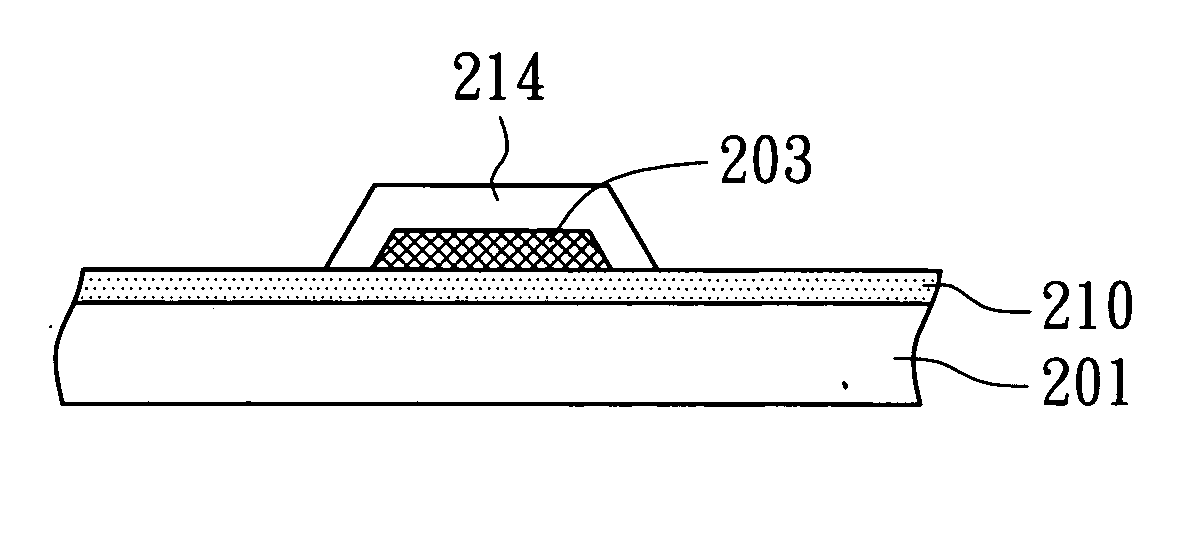
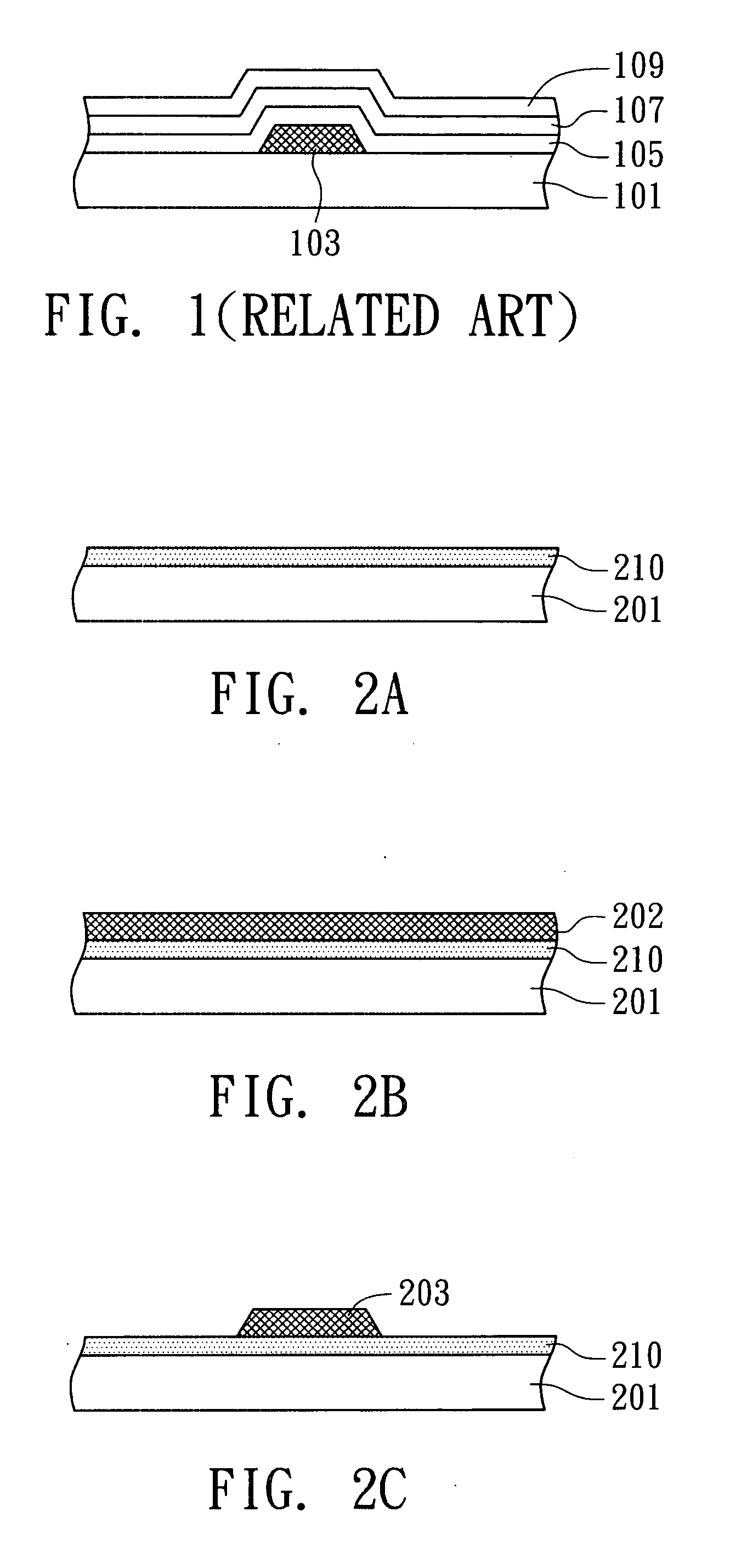
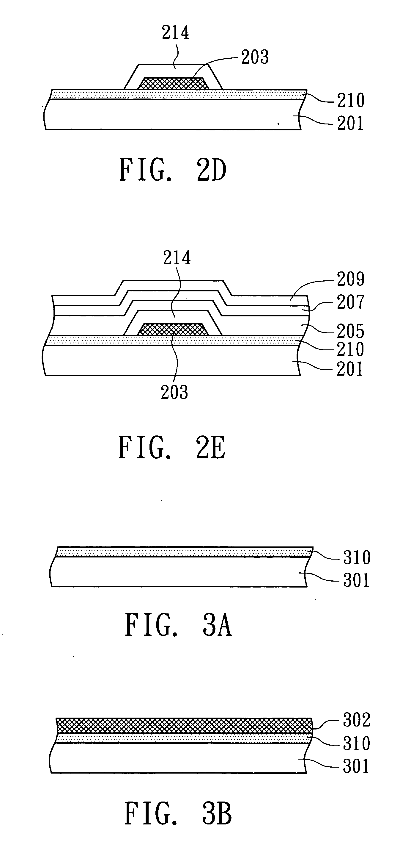
[0020]FIG. 2A˜FIG. 2E illustrate a partial process for fabricating a TFT-LCD according to the first embodiment of the invention. First, a glass substrate 201 pre-cleaned by deionized water is provided. An adhesion layer 210 is preferably formed on the glass substrate 201, as shown in FIG. 2A. The adhesion layer 210 could be formed by spin coating or spinless coating. The material of the adhesion layer 210 is the polymer comprising at least one of nitrogen and phosphorus, such as polysilane (with high transparency and thermal stability), photosensitive methylsilazane (PS-MSZ) and non-photosensitive MSZ (available from Clariant Cop.) The thickness of the adhesion layer 210 is ranged from about 100 nm to about 3000 nm.

[0021] Then, a copper layer 202 is formed (e.g. sputtered) on the adhesion layer 210, as shown in FIG. 2B. The copper layer 202 is then defined (i.e. patterned) by photolithography. For example, a photo-resist (PR) layer is formed above the copper layer 202, and the PR l...

second embodiment

[0026]FIG. 3A˜FIG. 3G illustrate a partial process for fabricating a TFT-LCD according to the second embodiment of the invention. First, a glass substrate 301 pre-cleaned by deionized water is provided. Then, an adhesion layer 310 is preferably formed on the glass substrate 301, as shown in FIG. 3A. The technique of spin coating or spinless coating could be used in the formation of the adhesion layer 310. The material of the adhesion layer 310 is the polymer comprising at least one of nitrogen and phosphorus, such as polysilane (with high transparency and thermal stability), photosensitive methylsilazane (PS-MSZ) and non-photosensitive MSZ (available from Clariant Cop.) The thickness of the adhesion layer 310 is preferably ranged from about 100 nm to about 3000 nm.

[0027] Then, a copper layer 302 is formed (e.g. sputtered) on the adhesion layer 310, as shown in FIG. 3B. The copper layer 302 is patterned by photolithography. For example, a photo-resist (PR) layer is formed above the ...


PUM

PropertyMeasurementUnit
thicknessaaaaaaaaaa
thicknessaaaaaaaaaa
thicknessaaaaaaaaaa

Abstract

A copper gate electrode, applied in a thin-film-transistor liquid crystal display (LCD) device, at least comprises a patterned copper layer formed on a glass substrate, and a barrier layer formed on the patterned copper layer. The barrier layer comprises at least one of nitrogen and phosphorus, or comprises an alloy formularized as M1M2R wherein M1 is cobalt (Co) or molybdenum (Mo), M2 is tungsten (W), molybdenum (Mo), rhenium (Re) or vanadium (V), and R is boron (B) or phosphorus (P).

Description

[0001] This application claims the benefit of Taiwan application Serial No. 93141259, filed Dec. 29, 2004, the subject matter of which is incorporated herein by reference. BACKGROUND OF THE INVENTION [0002] 1. Field of the Invention [0003] The invention relates in general to a copper gate electrode of liquid crystal display device and method of fabricating the same, and more particularly to the copper gate electrode having a barrier layer and the method of fabricating the same. [0004] 2. Description of the Related Art [0005] The thin film transistor liquid crystal displays (“TFT-LCD”), having the TFTs arranged in an array and the electrical components (i.e. capacitors, drivers), are capable of displaying the vivid images. With the advantages of handy size, light weight, low power consumption and no radiation contamination, the TFT-LCDs have been widely used in the world. In the commercial market, the TFT-LCD applications include the portable products such as personal digital assista...

Claims


Application Information

Patent Timeline
Patent Type & Authority Applications(United States)
IPC IPC(8): H01L29/40H01L21/44
CPCH01L29/4908
Inventor LIU, YU-WEITSAI, WEN-CHINGHUANG, KUO-YULIN, HUI-FEN
Owner AU OPTRONICS CORP
Why Eureka
Try Eureka