Process for producing high-resistance silicon wafers and process for producing epitaxial wafers and soi wafers (as amended)

a technology of high-resistance silicon and epitaxial wafers, which is applied in the direction of crystal growth process, after-treatment details, under a protective fluid, etc., can solve the problems of high cost of cmos circuit design, and high cost of rf-cmos circuit production, etc., to achieve the effect of reducing production costs

Active Publication Date: 2007-03-22
SUMCO CORP
View PDF7 Cites 15 Cited by
  • Summary
  • Abstract
  • Description
  • Claims
  • Application Information

AI Technical Summary

Benefits of technology

[0019] It is an object of the present invention, having been made in view of the above-discussed problems of the oxygen precipitation heat treatment to be applied in producing high-resistance wafers, to provide a process for producing high-resistance wafers which comprises subjecting high-resistance wafers grown by the CZ method with the addition of carbon to a preliminary heat treatment by a controll

Problems solved by technology

Since the RF characteristics attainable in the CMOS process were poor in the past, the cost of RF-CMOS circuit production was high, and the design of high-frequency circuits to be produced by the CMOS process has not been actively studied.
However, such substrates as GaAs-based ones are expensive from the production cost viewpoint and present problems when the wafer diameter is to be increased, and from the crystal defect controllability viewpoint, for instance, although they are excellent in RF characteristics.
Therefore, it is conceivable that silicon wafers be used as RF-CMOS circuit substrates but, generally, when silicon wafers with a resistance value of 10 Ωcm or below are used as circuit substrates, there is a limit to the improvement in performance characteristics of RF-ICs.
This is because, unlike digital circuits, RF circuits utilize on-chip inductor elements, highly fine capacitor elements and other analog passive elements and, in particular, the characteristics of inductors are greatly influenced by the parasitic effect of silicon wafer substrates; thus, the improvement in device performance characteristics by process refining alone is limited.
In the case of high-resistance wafers, however, the dopant level is low and the resistivity thereof is greatly influenced by the amount of oxygen donors generated.
However, the method based on the magnetic field application leads to an increase in production costs and, in addition, reportedly, the lower limi

Method used


Image

  • Process for producing high-resistance silicon wafers and process for producing epitaxial wafers and soi wafers (as amended)
  • Process for producing high-resistance silicon wafers and process for producing epitaxial wafers and soi wafers (as amended)
  • Process for producing high-resistance silicon wafers and process for producing epitaxial wafers and soi wafers (as amended)

Examples


example 1

[0132] For confirming the effects of the present invention, a crystal grown by the CZ method was processed into 8-inch p-type wafers having a resistivity of 2000 Ωcm, an initial interstitial oxygen concentration of 10 to 15×1017 atoms / cm3 (ASTM F 121-1979) and, further, a carbon concentration of 5×10¹⁶ atoms / cm3 (ASTM F 123-1981), and subwafers were prepared by subjecting the wafers to 1 hour of donor killer heat treatment at 650° C.

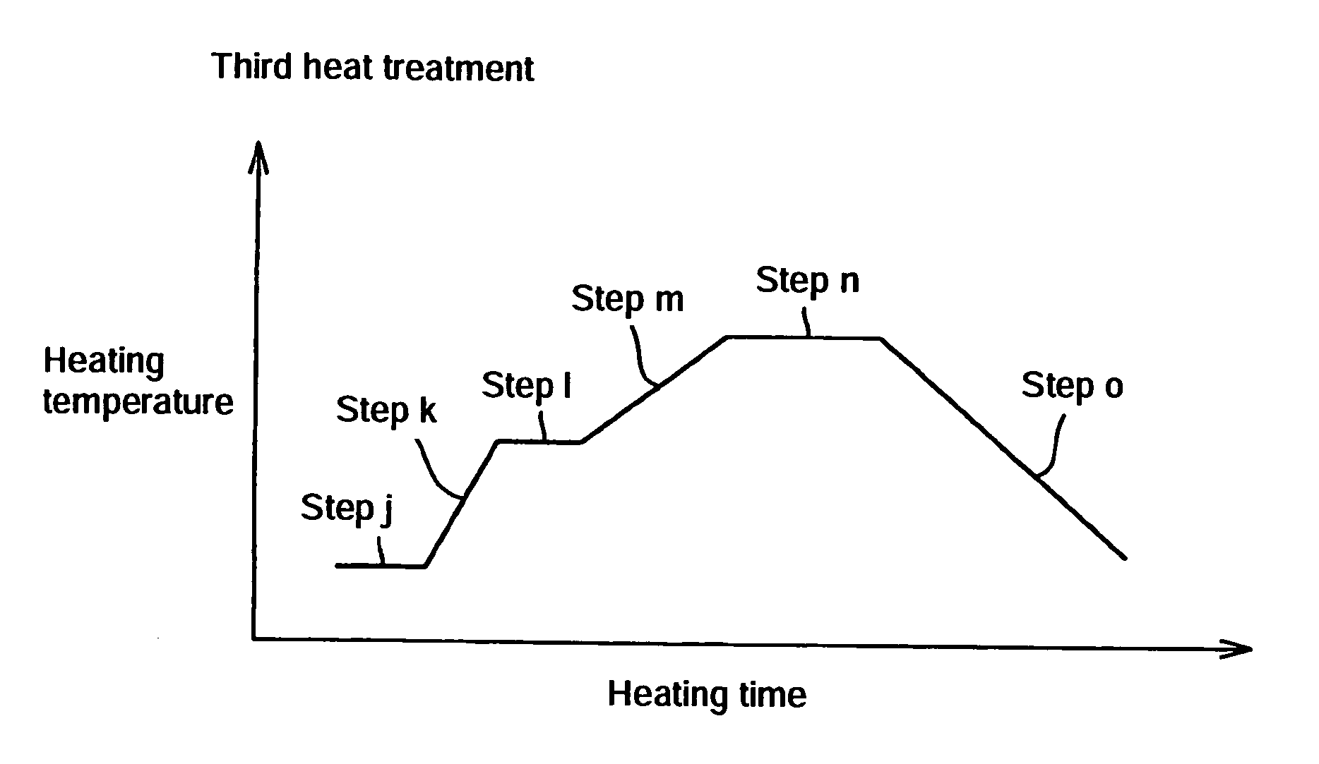
[0133] The subwafers prepared were subjected to first heat treatment, namely 1 hour of heat treatment at 900° C., following wafer charging in a furnace at a temperature of 700° C. and heating up at a rate of 1° C. / minute, using a N2 (containing 3% O2) gas atmosphere. Then, heat treatment was carried out, as second heat treatment, at 1200° C. for 1 hour using an Ar gas atmosphere. The temperature was then lowered to 1000° C., and heat treatment was carried out at that temperature for 10 hours.

[0134] The wafers obtained after the above heat treatment pro...

example 2

[0136] For confirming the effects of using wafers having a relatively high initial interstitial oxygen concentration, subwafers having a resistivity of 2000 Ωcm, an initial interstitial oxygen concentration of 13 to 15×1017 atoms / cm3 (ASTM F 121-1979) and, further, a carbon concentration of 5×10¹⁶ atoms / cm3 (ASTM F 123-1981) were prepared in the same manner as in Example 1 by carrying out donor killer heat treatment at 650° C. for 1 hour.

[0137] They were subjected to first heat treatment under the same conditions as in Example 1 and then to second heat treatment, namely 1 hour of heat treatment at 1200° C. in an Ar gas atmosphere and thereafter immediately discharged out of the furnace at 600° C. without subjecting to medium temperature treatment. The wafers obtained were subjected to silicon epitaxial growth treatment in a horizontal single wafer processing type growth furnace under the same conditions as in Example 1.

[0138] The epitaxial wafers obtained were examined for oxygen ...

example 3

[0139] Silicon wafers were produced in the same manner as in Example 1 by preparing 8-inch p-type subwafers having a resistivity of 2000 Ωcm, an initial interstitial oxygen concentration of 10 to 15×1017 atoms / cm3 (ASTM F 121-1979) and, further, a carbon concentration of 5×10¹⁶ atoms / cm3 (ASTM F 123-1981) and further subjecting them to first heat treatment and second heat treatment under the same conditions.

[0140] Using the thus-produced silicon wafers, oxygen ions were implanted into them from the front surface side at an acceleration voltage of 100 keV These wafers were placed in a heat treatment furnace maintained at 700° C., then heated to 1320° C. and maintained at that temperature for 10 hours. Thereafter, the wafers were cooled to 700° C. and discharged out of the furnace. SIMOX wafers were thus produced.

[0141] The SIMOX type SOI wafers obtained were subjected to 1 hour of heat treatment at 400° C. in an atmosphere of N2 (containing 3% O2) in a simulation of the heat treatm...


PUM


Abstract

By using oxygen-containing silicon wafers obtained by the CZ method and by combining the first heat treatment comprising controlled heat-up operation (ramping) with the second heat treatment comprising high-temperature heat treatment and medium temperature heat treatment in accordance with the process for producing high-resistance silicon wafers according to the present invention, it is possible to obtain high-resistance silicon wafers capable of maintaining their high resistance even after heat treatment in the process of device manufacture while efficiently inhibiting the formation of oxygen donors and preventing changes in resistivity. Further, excellent epitaxial wafers and SOI wafers can be produced using those high-resistance silicon wafers and, therefore, they can be applied in a wide field including high-frequency communication devices and analog/digital hybrid devices, among others.

Description

TECHNICAL FIELD [0001] This invention relates to a process for producing high-resistance silicon wafers to be used, for example, as base substrates for radio frequency communication devices or analog / digital hybrid devices, and to a process for producing epitaxial wafers and SOI (silicon-on-insulator) wafers using the high-resistance silicon wafers obtained by the process mentioned above. BACKGROUND ART [0002] As far as the CMOS process is concerned, low-cost RF-CMOS-LSIs for use in the RF (radio frequency) range have become realized with the rapid progress in RF characteristics of circuits. Significant applications thereof include, among others, transceiver ICs for portable devices, wireless LAN transceiver ICs suited for high speed, great capacity transmission, or analog / digital hybrid devices. [0003] Since the RF characteristics attainable in the CMOS process were poor in the past, the cost of RF-CMOS circuit production was high, and the design of high-frequency circuits to be pr...

Claims


Application Information

Patent Timeline
IPC IPC(8): H01L21/322C30B29/06C30B33/02H01L21/324H01L21/762
CPCC30B29/06C30B33/02H01L21/76243H01L21/324H01L21/322H01L21/20H01L27/12
Inventor KURITA, KAZUNARISADAMITSU, SHINSUKETAKAO, HIROYUKIHOURAI, MASATAKA
Owner SUMCO CORP
Why Eureka
Try Eureka