Semiconductor device and manufacturing method thereof

a semiconductor and manufacturing method technology, applied in the direction of semiconductor devices, basic electric elements, electrical equipment, etc., can solve the problems of increasing the number of steps, reducing the efficiency of the process, and reducing the number of manufacturing steps. , to achieve the effect of reducing material costs and personnel costs in the tft manufacturing, and reducing the number of manufacturing steps

Inactive Publication Date: 2007-08-09
SEMICON ENERGY LAB CO LTD
View PDF48 Cites 47 Cited by
  • Summary
  • Abstract
  • Description
  • Claims
  • Application Information

AI Technical Summary

Benefits of technology

[0020] In view of the above problems, the present invention intends to find a method of manufacturing a TFT substrate at low costs. That the number of steps is numerous is at the heart of the problem; accordingly, how to reduce the number of steps is considered. In order to reduce the indispensable steps in the manufacture of the TFT, it is necessary to reconsider a TFT structure itself and to reconstruct a manufacturing process thereof.
[0021] Accordingly, the invention intends to proposes a novel TFT structure and a novel process for manufacturing the novel TFT structure to largely reduce TFT manufacturing steps, and thereby to largely reduce the manufacturing cost of a TFT substrate. Furthermore, the invention intends to reduce a photolithography process and thereby to reduce the number of masks that are used in the TFT manufacturing process. (Means for Solving the Problems)
[0032] Furthermore, in the above configuration according to the invention, a thin film transistor of a semiconductor device includes a semiconductor film including a channel formation region, and as the semiconductor film a microcrystalline semiconductor can be used. The microcrystalline semiconductor is a film including a semiconductor that has a structure intermediate between an amorphous and a crystalline structure (including single crystal and poly crystal). The microcrystalline semiconductor is a semiconductor that has a third state that is stable from a free energy point of view, crystalline one that has a short-range order and lattice distortion, and one that is allowed to exist dispersed in a non single crystalline semiconductor when a particle diameter thereof is in the range of 0.5 to 20 nm. In the microcrystalline semiconductor, a Raman spectrum thereof is shifted toward a lower frequency side than 520 cm−1, and, in X-ray diffraction, diffraction peaks of (111) and (220) that are said owing to a Si crystal lattice are observed. Furthermore, hydrogen atoms or halogen atoms as a neutralizer of the dangling bonds are contained 1 atomic percent or more. For convenience sake, such a semiconductor is called a semi-amorphous semiconductor (SAS). Furthermore, when a rare gas element such as helium, argon, krypton or neon is contained and thereby the lattice distortion is further forwarded to increase the stability, an excellent semi-amorphous semiconductor can be obtained.
[0043] When a TFT structure that does not have an interlayer insulating film is adopted, a process can be largely simplified. Furthermore, a string of steps including forming a contact hole and establishing an electrical connection becomes unnecessary. Still furthermore, owing to a decrease in the number of manufacturing steps, material costs and personnel costs in the TFT manufacture decrease, resulting in realizing low costs. The number of devices becomes less and steps that use a vacuum can be largely reduced; accordingly, equipment investment becomes less. Furthermore, a manufacturing time period up to the completion of a TFT can be also largely shortened.
[0044] According to the configuration according to the invention, since apparatus can be easily enlarged, the present invention can be preferably applied to the manufacture of a semiconductor device such as a display device that uses a larger size substrate. Furthermore, since the number of steps is very small, yield can be improved.

Problems solved by technology

However, as to TFT substrates, the effort to reduce the cost is belated.
Accordingly, high manufacturing costs and personnel costs are necessary.
That is, since interconnections are formed into a multi-layered structure to realize cubic crossings, contact holes are necessary to be formed, resulting in an increase in the number of steps.
In this case also, a TFT has to be formed according to a complicated manufacturing process that makes use of photolithography; accordingly, there is a problem similar to that in the TFT that uses a polycrystalline silicon film.

Method used


Image

  • Semiconductor device and manufacturing method thereof
  • Semiconductor device and manufacturing method thereof
  • Semiconductor device and manufacturing method thereof

Examples


embodiment mode 1

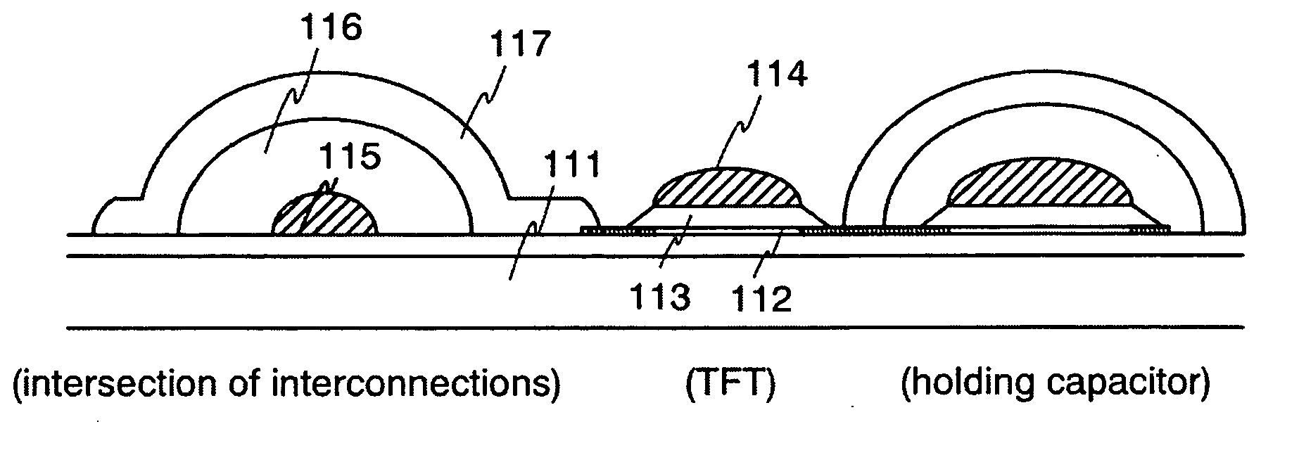
[0055] With reference to FIG. 1 a specific method of manufacturing a TFT according to the invention will be explained. When a TFT structure according to the invention is adopted, in comparison with a conventional method shown in FIG. 7, the number of steps can be largely reduced.

[0056]1. Formation of active layer

[0057]2. Source / drain doping

[0058]3. Successive formation of gate insulating film, gate electrode and gate interconnection, source interconnection and holding capacity

[0059] Firstly, on a substrate 111, an island-like semiconductor layer 112 that becomes an active layer is formed. The substrate 111 is made of various kinds of materials such as glass, quartz, semiconductor, plastics, plastics film, metal, glass epoxy resin and ceramics. A substrate made of a flexible synthetic resin such as plastics, though having general tendency to be low in the heat resistance temperature compared with glass and metal, as far as it can stand a processing temperature in a manufacturing ...

embodiment mode 2

[0078] On the occasion of manufacturing a semiconductor device with a substrate having the translucency in the present embodiment mode according to the invention, as a size of substrate, a large size substrate such as 600 mm×720 mm, 680 mm×880 mm, 1000 mm×1200 mm, 1100 mm×1250 mm, 1150 mm×1300 mm, 1500 mm×1800 mm, 1800 mm×2000 mm, 2000 mm×2100 mm, 2200 mm×2600 mm, or 2600 mm×3100 mm is used.

[0079] When such a large size substrate is used, the manufacturing cost can be reduced. As the substrates that can be used, substrates made of glass such as barium borosilicate glass or aluminoborosilicate glass typical in Corning #7059 glass and #1737 glass can be used. Furthermore, as other substrates, various kinds of translucent substrates such as quartz, semiconductor, plastics, plastics film, metal, glass epoxy resin, and ceramics can be used as well.

embodiment mode 3

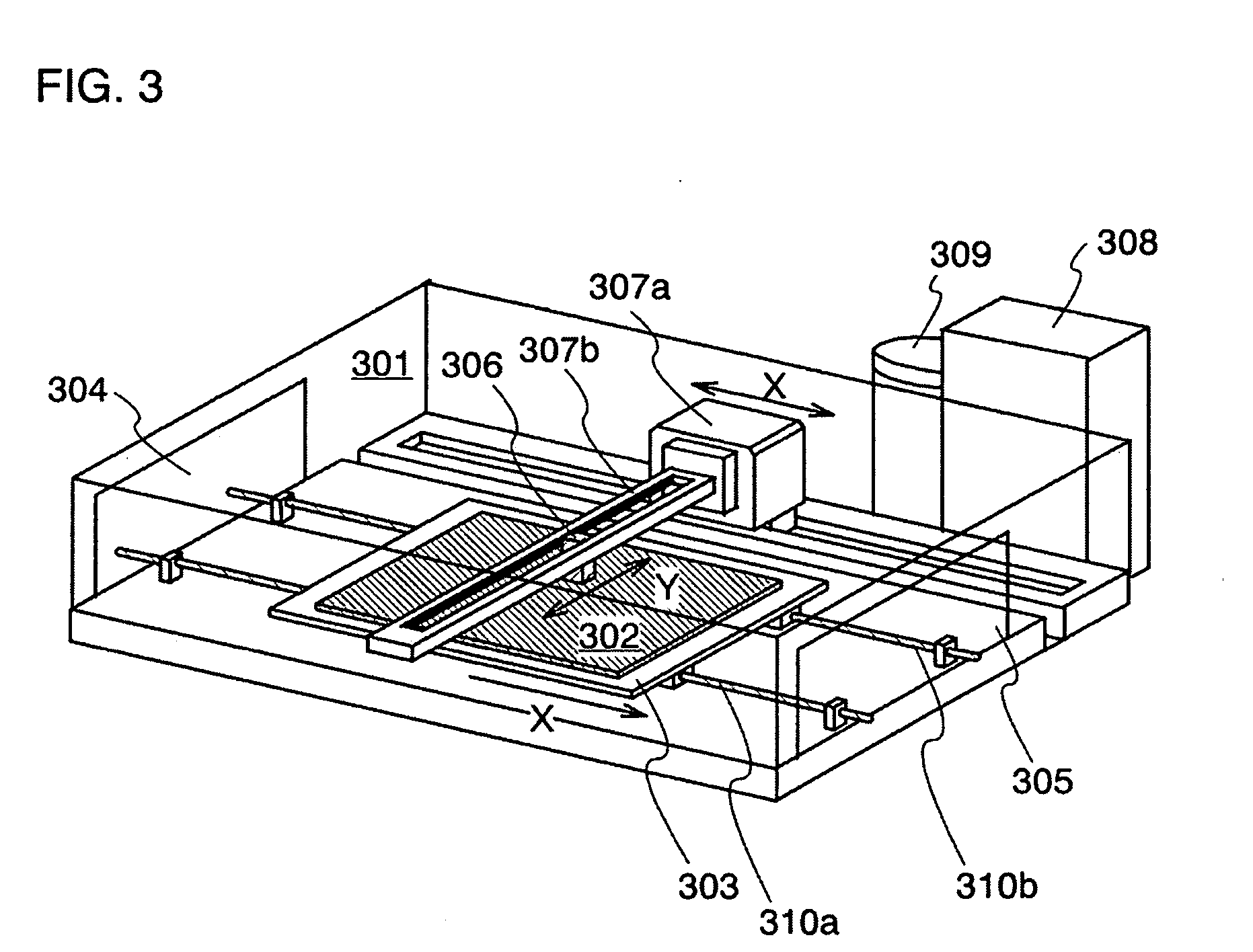
[0080] An example of a liquid drop discharge device that is used for carrying out the embodiment mode will be explained with reference to FIGS. 3 to 5.

[0081] A liquid drop discharge device shown in FIG. 3 has a liquid drop discharge means 306 in the device, by use of which a solution is discharged, and thereby a desired pattern is obtained on a substrate 302. In the liquid drop discharge device, as the substrate 302, other than a glass substrate having a desired size, subjects to be processed such as a resinous substrate typical in a plastics substrate or a semiconductor wafer typical in silicon can be used.

[0082] In FIG. 3, the substrate 302 is carried from an inlet port 304 into a chassis 301, and a substrate undergone a liquid drop discharge step is carried out of an outlet port 305. Inside ofthe chassis 301, the substrate 302 is mounted on a transfer table 303 and the transfer table 303 moves on rails 310a and 310b that connect between the inlet port and the outlet port.

[0083...


PUM


Abstract

An island-like interlayer insulating film is formed selectively in a region where a source interconnection and a gate interconnection intersect. For example, by use of ink jet method, a solution containing an insulating material is dropped on a region where the gate interconnection and the source interconnection intersect or a region where a holding capacitor is formed, that enable to reduce a photolithography process and to reduce the number of masks that are used in a TFT

Description

TECHNICAL FIELD [0001] The present invention relates to a method of manufacturing a semiconductor device, in particular, a semiconductor device that has a circuit constituted of an active matrix type field effect thin film transistor (hereinafter, referred to as a TFT) on a substrate having an insulating surface and a method of manufacturing the same. BACKGROUND ART [0002] In recent years, large size liquid crystal display devices are gathering attention and vigorous efforts are being forwarded to realize low cost liquid crystal panels. However, as to TFT substrates, the effort to reduce the cost is belated. On the occasion of forming an image display element in a liquid crystal display device, a lot of manufacturing steps such as a deposition step, an etching step, a doping step, a washing step, a photolithography step, an ashing step and a heat treatment step are necessary. Accordingly, high manufacturing costs and personnel costs are necessary. [0003] A reason for that a manufact...

Claims


Application Information

Patent Timeline
Patent Type & Authority Applications(United States)
IPC IPC(8): H01L27/12H01L21/336H01L21/768H01L21/77
CPCH01L27/12H01L29/66742H01L27/1292H01L27/1248H01L27/1285H01L27/124
Inventor NAKAMURA, OSAMU
Owner SEMICON ENERGY LAB CO LTD
Why Eureka
Try Eureka