

Positively radiation-sensitive resin composition
a radiation-sensitive, resin technology, applied in the direction of solid-state devices, basic electric elements, electrical appliances, etc., can solve the problems of low production efficiency, prolonged exposure time, and inability to obtain a pattern having a perpendicular sidewall, and achieve excellent sensitivity and resolution, accurate transfer, and excellent resolution performance
- Summary
- Abstract
- Description
- Claims
- Application Information
AI Technical Summary
Benefits of technology
Problems solved by technology
Method used
Image


Examples
synthesis example 1
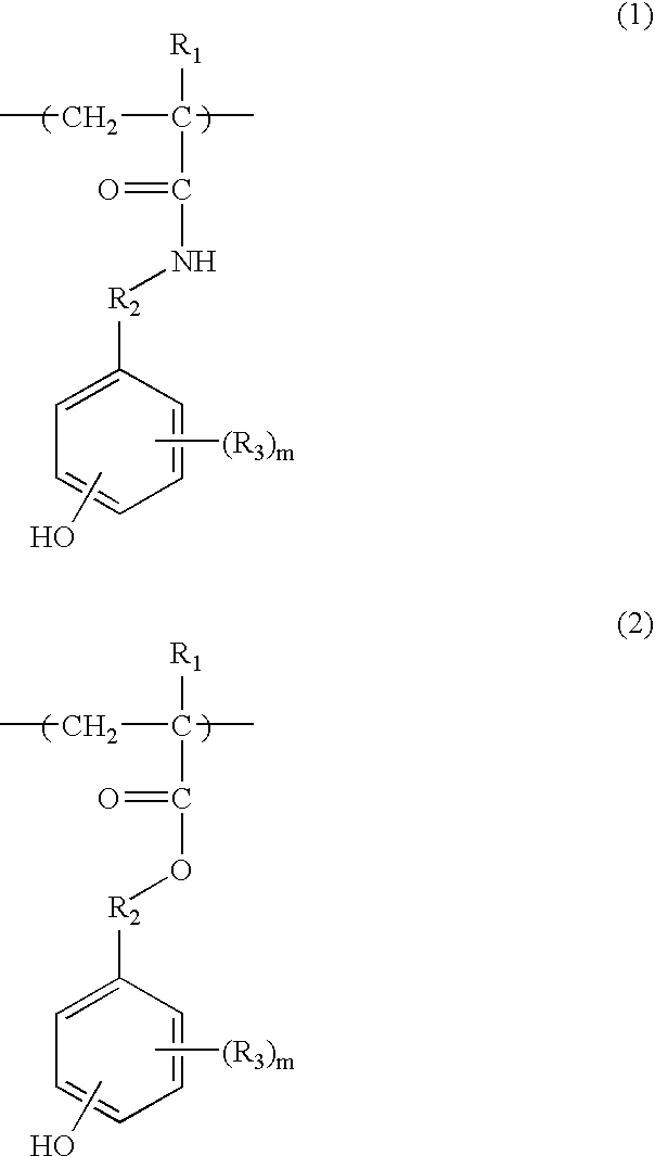
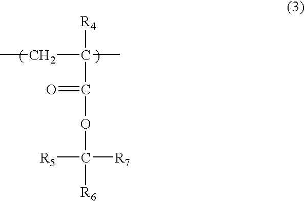
[0146] 20 g of p-hydroxyphenyl methacrylamide, 20 g of p-isopropenylphenol, 20 g of 2-hydroxyethyl acrylate, 20 g of isobornyl acrylate and 30 g of 2-benzyl-2-propyl methacrylate were mixed with 150 g of ethyl lactate, and the mixture was stirred at 50° C. to give a homogeneous solution. After a nitrogen gas was bubbled through the solution for 30 minutes, 4 g of AIBN was added. With continuing bubbling of a nitrogen gas and maintaining the reaction temperature at 70° C., polymerization was carried out for 7 hours. After the polymerization was completed, the reaction solution was mixed with a large amount of hexane to solidify the resulting polymer. Subsequently, the polymer was redissolved in tetrahydrofuran and then solidified by the use of hexane again. These operations were repeated several times to remove the unreacted monomers, and the resulting polymer was dried at 50° C. under reduced pressure to obtain a white polymer A1.
synthesis examples 2 to 10
[0147] Copolymers A2 to A10 were synthesized in the same manner as in the synthesis of the copolymer A1 of Synthesis Example 1, except that the types and the amounts of the compounds were changed in accordance with compositions of Table 1. Further, copolymers A11 to A25 were synthesized in the same manner as in the synthesis of the copolymer A1 of Synthesis Example 1, except that the solvent used was changed to propylene glycol monomethyl ether acetate.
Synthesis of Polymer for Comparison
synthesis example 11
[0148] 30 g of p-isopropenylphenol, 20 g of 2-hydroxyethyl acrylate and 50 g of 2-benzyl-2-propyl acrylate were mixed with 150 g of ethyl lactate to give a homogeneous solution. After a nitrogen gas was bubbled through the solution for 30 minutes, 4 g of AIBN was added. With continuing bubbling of a nitrogen gas and maintaining the reaction temperature at 70° C., polymerization was carried out for 7 hours. After the polymerization was completed, the reaction solution was mixed with a large amount of hexane to solidify the resulting polymer. Subsequently, the polymer was redissolved in tetrahydrofuran and then solidified by the use of hexane again. These operations were repeated several times to remove the unreacted monomers, and the resulting polymer was dried at 50° C. under reduced pressure to obtain a white polymer R1.
PUM
| Property | Measurement | Unit |
|---|---|---|
| thickness | aaaaa | aaaaa |
| height | aaaaa | aaaaa |
| boiling point | aaaaa | aaaaa |
Abstract
Description
Claims
Application Information